Spot Issues Early: Optimize PCB Design with DFM Inspection
Maximize Efficiency with Thorough DFM Inspection
- Improves design quality, preventing potential issues
- Detects design flaws early, reducing testing costs
- Enhances PCB assembly manufacturability
- Simplifies the revision process, shortening cycles
- Reliable, On-Time Delivery for Your PCB assembly Orders
DFM Inspection
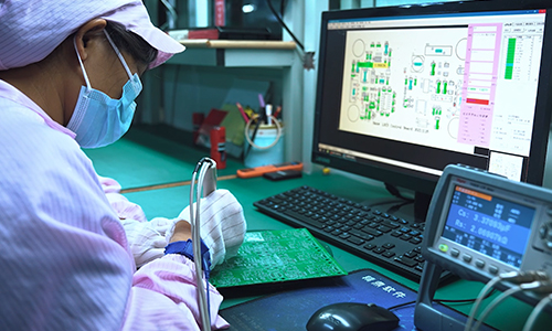
PCBA DFM Inspection
SCSPCBA is committed to providing global customers with samples and one-stop electronic manufacturing services for small and medium batches. PCBA DFM inspections can be performed by SCSPCBA to ensure your PCBs are manufactured correctly and increase the reliability of your products.
Before PCBA production, we will conduct a DFM inspection on customer design documents to ensure the quality of the manufacturing process, provide professional DFM reports, and may partially modify the design.

Principles of DFM for PCB Design
- Minimize Complexity
Simplifying the PCB board design helps streamline the circuit board manufacturing process and reduces potential errors. For instance, using fewer electronic components or reducing the number of PCB board layers can lower costs and improve yields.
- Design for Ease of Assembly
Components should be placed in positions that are easy to access during electronic assembly. Circuit boards and components should be oriented for automated assembly and soldering, reducing labor costs and minimizing errors.
- Standardization of Components
Using commonly available components and standard footprints minimizes procurement costs and ensures a smoother PCB board fabrication process. Avoiding proprietary or rare components can prevent delays due to electronic parts shortages or lead time issues.
- Manufacturability of Vias and Holes
The use of vias, through-holes, and blind or buried vias should be considered carefully to prevent complications during printed circuit board production. Excessive or improperly placed vias can lead to increased costs and reduced reliability.
- Design for Testability
Test points should be incorporated in the PCB design to facilitate efficient testing during manufacturing. Accessible PCB test points allow for quick fault detection and can prevent costly production delays due to undetected defects.
- Minimize printed circuit board layers Count
A multilayer PCB board design is more expensive and complex to manufacture. Whenever possible, aim for a design with fewer layers, as this simplifies the production process and reduces cost.
- Ensure Proper Signal Integrity
DFM principles also involve ensuring that signal integrity is maintained throughout the PCB layout design. Proper routing of signal traces, impedance control, and grounding techniques can help prevent signal degradation and interference.
Key DFM Considerations for PCB Design
- Trace Width and Spacing
Traces that are too narrow or too close to each other can lead to electrical short circuits or failed boards. Standardized trace widths and spacing help printed circuit board manufacturers avoid errors and defects.
- Component Placement
Components should be arranged in a logical order, making it easier for automated assembly equipment to pick and place parts accurately.
- Pad and Via Design
Use larger pad sizes for electronic components with higher pin counts and ensure vias are properly designed to avoid causing impedance mismatches or pc board assembly defects.
- Use of Solder Mask
The application of solder mask helps to prevent shorts and damage to the circuit board. Careful design of the solder mask layers ensures proper coverage, especially around fine-pitch components and via holes.
- Copper Thickness
The thickness of the copper used in the PCB affects both electrical performance and the manufacturability of the board. Ensure that copper thicknesses are suitable for the expected current load and are achievable within the chosen circuit board manufacturing process.
- Panelization
Panelization involves grouping multiple PCBs on a single production panel. Proper panelization minimizes material waste and reduces production time.
- Design for Reliability
A key goal of DFM is ensuring the long-term reliability of the circuit board. Considerations such as avoiding sharp corners, ensuring appropriate hole drilling, and using proper component packaging help increase the overall lifespan of the board and reduce failure rates.
- Cost Considerations
While designing for performance, it’s crucial to keep cost-effective manufacturing in mind. This includes choosing readily available components, designing the PCB to minimize material waste, and choosing manufacturing processes that balance cost with quality.
Benefits of Implementing DFM
Design for Manufacturing (DFM) is an essential approach for optimizing PCB design and ensuring cost-effective, high-quality production.
By adhering to DFM principles, designers can avoid potential pitfalls, streamline production, and create PCBs that meet performance and reliability requirements. Key factors such as component placement, trace design, and manufacturability should always be considered to reduce costs, prevent errors, and improve time-to-market. Embracing DFM in PCB design is not just about making products easier to manufacture, but also about creating designs that are robust, efficient, and cost-effective throughout their lifecycle.
AI Intelligent Online Quotation
Recommended Services


