Get High-quality Circuit Board Services at Affordable Prices
PCB Design
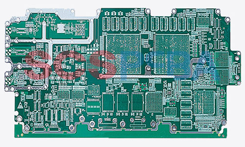
PCB design includes creating a printed circuit board layout, including schematic capture, electronic component placement, electrical connection routing, and circuit design rule checking.
☑ ISO9001 & UL Certified
☑ PCB board design experts
☑ Accurate and fast quotation
☑ Join us to get PCB design services
☑ Intelligent circuit board manufacturing factory
PCB Design
Three Methods in Designing Circuit Board
- Manual PCB Design
Manual PCB layout is designed manually using pen and paper, or specialized PCB manufacturing software. Manual circuit design is suitable for small and simple designs but is time-consuming and error-prone.


- Automatic PCB Board Design
It is the method of automatically routing connections on a PCB layout using software. This approach saves time and effort in designing large and complex boards. - Hybrid PCB Design Approach
The hybrid approach combines circuit board manual design and PCB board automatic routing.
SCSPCBA professional PCB designers team manually places critical electronic circuit board components and routes high-speed and sensitive connections while routing the rest using the auto-routing function.
Streamlined Printing Circuit Board Drawing
PCB schematic diagram design is a visual representation of a printed circuit board and its components. It usually includes information such as the location, orientation, and polarity of electronic circuit board components.
- Component Placement
The diagram will show the location and orientation of each electronic part on the board. - Printed Circuit Board Layout
It will show the PCB layout, including the locations of traces, vias, and mounting holes. - PCB Soldering
The PCB diagram includes information such as recommended soldering temperature, amount of solder to use, and duration of the soldering process.
- Test Point
Test points on the PCB board can be used to check the functionality of the circuit board during the testing phase.
Overall, printed circuit assembly drawing is a useful tool in ensuring that the circuit PCB board is assembled and functioning properly.
How to Get Started with PCB Board Design
Starting a PCB design project can seem daunting, but it can be an enjoyable and rewarding experience if approached the right way. Here are the steps to start basic circuit board design.
- Define Project Requirements
Define Project Requirements, including the Purpose of circuit boards, the types of electronic components, and size and shape. - Choosing PCB Design Software
PCB design software options include Eagle, Altium Designer, and KiCad. - Creating A Schematic
The schematic is the first step in designing a PCB. It shows the connections between circuits and components and helps identify any potential design issues.
- Create the PCB Layout
Placing electronic components on the PCB circuit board and routing connections between them. - Verify Design
Before sending design files for PCB board fabrication, it is important to verify the circuit design for any errors or issues, such as design rule checking (DRC). - Generate Manufacturing Files
Generate circuit board manufacturing files including Gerber files, which contain the printed circuit board design information.
- Send Files for Fabrication
Finally, the fabrication files are sent to the PCB manufacturer for production.
Remember, circuit board design is a skill that takes time to develop. Don’t be afraid to ask for help or consult online resources and forums to improve your skills.
Is PCB a CAD design?
Yes, PCB design is a type of CAD (Computer Aided Design) software used to design electronic circuits and printed circuit boards. circuit design software allows designers to create schematics, define board layouts, and perform routing to connect the various components on the board. PCB design software also provides tools for validating designs, generating manufacturing files, and interacting with PCB manufacturers. So, circuit board design is a specific type of CAD design that focuses on designing and manufacturing printed circuit boards.
AI Intelligent Online Quotation
Recommended Services


