Enhances PCB Performance Reduces Production Costs
What Is Via in Pad
Via in Pad is a technology commonly used in printed circuit board design, which allows the pins of electronic components to be directly connected to the vias located in pad. It provides a more compact and reliable connection method.
☑ Via-in-pad design improves circuit board density
☑ Widely compatible design, adaptable to a variety of high-end devices
☑ Enhanced vibration resistance and improved circuit board durability
☑ Optimizes signal transmission path and reduces PCB circuit signal loss
☑ Simplifies multi-layer board design and adapts to complex PCB board fabrication requirements
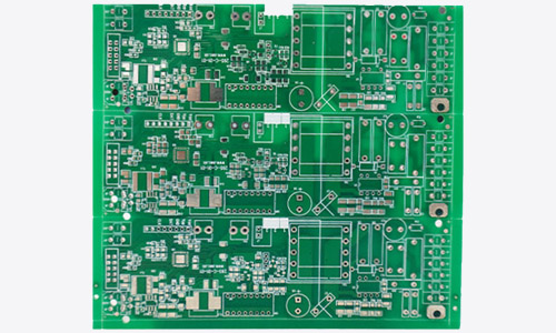
VIA IN PAD PCB
Cost-Effective VIA IN PAD PCB Manufacturing
- Reduce the number of pads: The number of electronic component pins can be reduced by embedding via holes in the pads. This is particularly important for high-density and small-sized PCB designs.
- Improve signal integrity: Reduce pin length and circuit paths by connecting the pins directly to the via holes in pads, resulting in reduced signal delay and interference.


- Improve thermal management: The Via in Pad process can also be used for thermal management. Heat can be conducted and dispersed more effectively by placing a thermal pad or heat sink in the pad.
- Improve reliability: Hole-in-pad process can provide more reliable pin connection. The mechanical stress and strain on the pins is reduced by connecting the pins directly to the pads, thereby reducing the risk of pins breakage or detachment.
The via-in-pad PCB board fabrication increases manufacturing costs because it requires more complex manufacturing process and specialized production equipment. SCSPCBA is a professional manufacturer for Via-in-Pad PCB, providing you with the perfect printed circuit board assembly solutions.
AI Intelligent Online Quotation
Recommended Services


