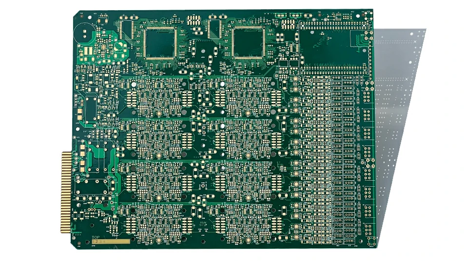
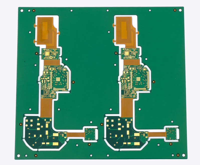
Ultra-High-Layer PCB (16-50 Layers)

Ultra-High-Layer PCB Manufacturing Process

Material Selection – Choosing high-quality laminates that can handle multiple layers and provide thermal stability.

Layer Stacking – Precision alignment of copper foils, prepreg, and core materials to form each layer.

Lamination – Applying high temperature and pressure to bond the layers into a solid structure.

Drilling & Plating – Micro-drilling for vias and plating to establish electrical connections between layers.

Etching & Imaging – Advanced etching techniques create precise circuit patterns on each layer.

Testing & Inspection – Rigorous electrical, mechanical, and thermal testing ensures reliability for complex, high-performance applications.

Manufacturing Features of Ultra-High-Layer PCB

Ultra-high-layer PCBs, typically exceeding 30 layers, require advanced manufacturing techniques like sequential lamination, laser drilling, and precise impedance control. They offer high-density interconnects, excellent signal integrity, and superior reliability for complex applications. SCSPCBA specializes in producing ultra-high-layer PCBs with optimized stack-up designs, ensuring durability, electrical performance, and thermal management for aerospace, telecommunications, and high-performance computing industries.

Application Fields of Ultra-High-Layer PCB

Ultra-high-layer PCBs are widely used in cutting-edge industries requiring high performance, signal integrity, and thermal management, including:

Telecommunications & Networking: 5G base stations and high-speed data centers, High-frequency RF communication systems, Optical fiber transmission equipment

Aerospace & Defense: Avionics and military radar systems, Spacecraft communication modules, Missile guidance and satellite systems

Medical Equipment: MRI and CT scan imaging systems: Advanced diagnostic and monitoring devices

Automotive & Electric Vehicles: Advanced driver-assistance systems (ADAS), LiDAR and radar sensors for autonomous driving, Electric vehicle (EV) power distribution modules

Industrial & AI Computing: High-performance computing (HPC) systems, AI servers and quantum computing processors, Embedded computing and robotics

SCSPCBA’s Ultra-High-Layer Circuit Board Manufacturing Capabilities

PCB Board Fabrication Capabilities
Ultra-High-Layer PCB ItemUltra-High-Layer PCB Capability
Number of Layers

16 – 50+ layersSurface Finishes ENIG, Immersion Silver, Immersion Tin, OSP, HASL, Lead-free HASL
Max Board Size
610mm × 1200mm (custom sizes available)Solder Mask Colors Green, Blue, Black, White, Red, Yellow
Min Board Thickness 1.0mmImpedance Control Yes, with advanced simulation and strict tolerance (±5%)
Max Board Thickness 12.0mmThermal Management Thermal vias, heat sinks, metal core options available
Base Materials FR4 (High-Tg), Rogers, PTFE, Polyimide, CeramicWarping Tolerance ≤0.5%
Copper Thickness 0.5oz (18µm) to 6oz (210µm)Hole Copper Thickness ≥25µm
Min Line Width/Spacing 0.075mm/0.075mm (3mil/3mil)
Testing Methods Flying probe, X-ray inspection, AOI, impedance test, high-voltage test, thermal cycling
Min Drilled Hole Diameter 0.2mm (8mil) for mechanical drilling, 0.075mm (3mil) for laser drillingSize Tolerance
≤±50μm

AI Intelligent Online Quotation

PCB Services

PCBA Service

BOM Services

Recommended Services

PCB Fabrication Services

Components Services

PCB Assembly Services

Box Build Assembly Cases

Solution Development

©Copyright 2025 SCS | All Rights Reserved |