Circuit Board Manufacturing Essentials: Complete SMT Production Line Analysis
In modern electronic product manufacturing, the surface mount technology (SMT) production line is the core link of printed circuit board assembly. A complete SMT production line can realize efficient and accurate electronic component placement to meet various products’ manufacturing needs, from consumer electronics to industrial equipment.
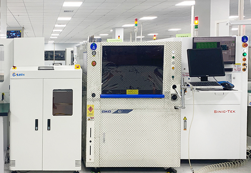
1. Fully Automatic Printing Machine
A fully automatic printing machine is the first process of SMT production line, responsible for accurately printing solder paste onto the pads of PCB. High-end printing machine has the following features:
- High-precision scraper system: adopts double scraper design, pressure, speed and angle can be precisely controlled
- Visual alignment system: realize accurate alignment between circuit board and steel mesh through high-resolution camera
- Automatic cleaning function: clean steel mesh regularly to prevent solder paste residue from affecting printing quality
- Real-time monitoring: monitor parameters such as pressure and speed during printing to ensure consistency
2. SPI Solder Paste Inspection System
The solder paste inspection (SPI) system uses 3D inspection technology to conduct a comprehensive inspection of the thickness, volume, area and shape of the solder paste, and can detect:
- Insufficient or excessive solder paste
- Solder paste bridging
- Solder paste position offset
- PCB board production poor shape and other problems
The SPI system greatly reduces the subsequent circuit board manufacturing process problems caused by poor solder paste printing. It is an indispensable part of high-quality surface mounting technology production lines.
3. High-speed and High-precision Placement Machine
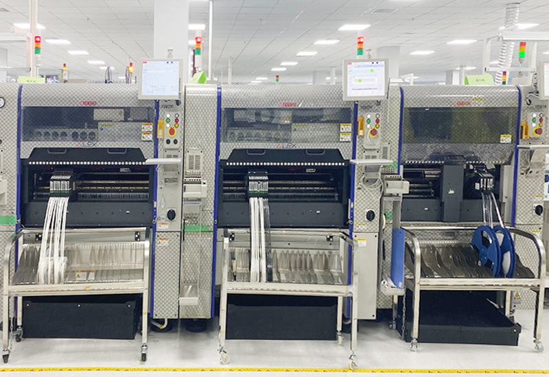
The placement machine is the core equipment of the SMT production line, responsible for removing electronic components from the feeder and accurately placing them on the designated position of the PCB boards. The placement machine has the following characteristics:
- Ultra-high speed: some models can reach more than 150,000 points per hour
- Multi-type component processing: from 01005 tiny components to large QFP, BGA, etc.
- High precision: placement accuracy can reach ±25μm @3σ
- Intelligent feeding system: supports component feeding in various packaging forms
- Real-time calibration: advanced functions such as flying focus and component height detection
High-end production lines are equipped with multiple placement machines to form a “patch island” to achieve the optimal allocation and highest efficiency of different types of components.
4. Automatic Optical Inspection (AOI)
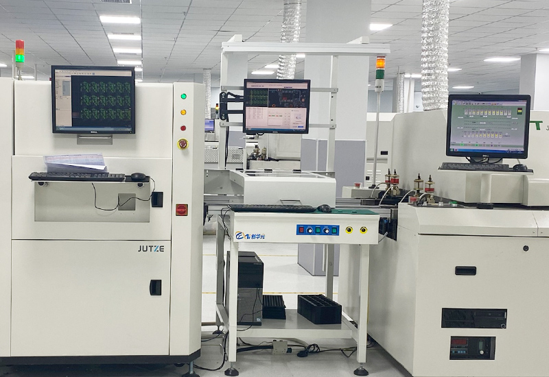
After the patch process, AOI (Automatic Optical Inspection) conducts a comprehensive appearance inspection of the PCB board, mainly inspecting:
- Missing components: Check whether there are missing components
- Polarity error: Identify whether the direction of polarized components is correct
- Position offset: Measure the deviation between the actual position of the element and the designed position
- Component error: Check whether the component value is consistent with the design requirements
The AOI equipment uses multi-angle lighting and high-resolution cameras, inspect the soldering quality and component placement accuracy on the printed circuit assembly, ensuring defect-free assemblies to achieve extremely high detection accuracy and extremely low false alarm rate.
5. Nitrogen Reflow Soldering Furnace
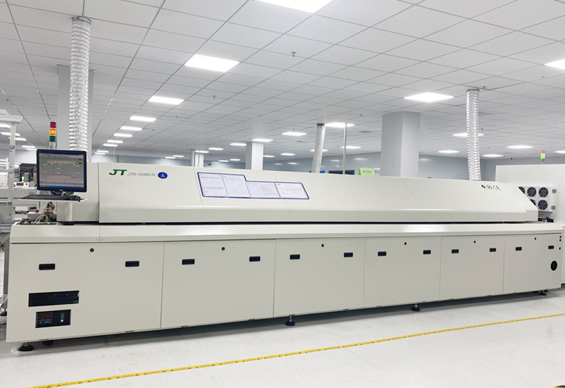
Reflow soldering is a key process to fix the mounted components on the circuit board by heating. Nitrogen reflow oven is the most advanced reflow soldering equipment at present, and its main features include:
- Multi-temperature zone precision control: usually 8-12 temperature zones, each temperature zone can be independently controlled
- Nitrogen protection environment: reduce oxidation and improve PCB manufacturing welding quality
- Hot air and infrared mixed heating: ensure PCB board fabrication temperature uniformity
- Real-time temperature monitoring: monitor the actual temperature curve of PCB through thermocouples
- Cooling system: rapid cooling to form good solder joints
Nitrogen environment can significantly reduce solder joint oxidation, especially suitable for welding high-density and fine-pitch components, and improve printed circuit board assembly reliability.
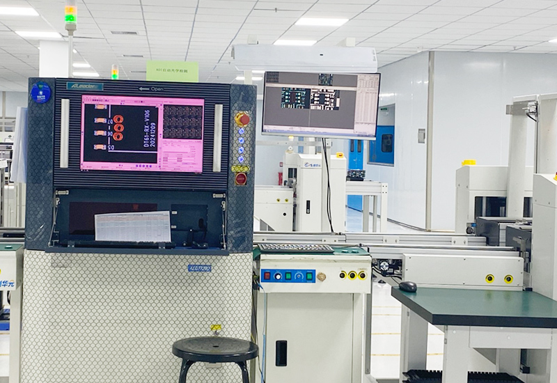
6. Final AOI: Automatic Optical Inspection
The final AOI inspection after reflow soldering is the last quality checkpoint of the SMT production line. The main inspections are:
Welding quality: whether the solder joints are complete, insufficient tin, excessive tin, cold solder joints, etc.
Component status: whether the components are damaged or shifted after reflow soldering, etc.
Bridge short circuit: check whether there is a tin bridge between adjacent solder joints
Contamination inspection: check whether there are foreign objects or contamination on the board
The advanced final AOI system can perform 3D solder joint inspection, combined with AI algorithms, to identify various complex welding defects.
7. Integration of Auxiliary Systems and Production Lines
The complete SMT production line also includes the following auxiliary systems:
Automated logistics system: an automatic conveyor connecting each process
MES production execution system: monitors and manages the entire production process
Data collection and analysis system: collects data from each process for quality analysis and traceability
Environmental control system: maintains constant temperature, humidity and cleanliness in the workshop
8. Analysis of SCSPCBA’s Complete SMT Production Line
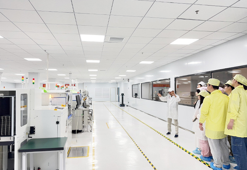
The fully equipped high-end SMT production line can significantly improve the efficiency, precision, and yield of PCB manufacturing, bringing the following core competitive advantages to SCSPCBA printed circuit board manufacturers:
★ Ultra-high Production Efficiency and Reduced Manufacturing Costs
The fully automatic printer, high-speed placement machine (CPH>150,000) and intelligent logistics system work together to achieve unmanned continuous production, greatly increase production capacity, and reduce circuit board production costs.
★ Extreme Precision Supports High-density Printed Circuit Assembly
±25μm placement accuracy, SPI solder paste detection and AOI intelligent detection system ensure the reliable placement of precision devices such as 01005 micro components and 0.3mm pitch BGA, meeting the needs of high-precision PCBs such as 5G and AI chips.
★ Nitrogen Reflow Soldering Improves Soldering Yield
Nitrogen protects the environment and reduces oxidation, and cooperates with multi-temperature zone precise temperature control to reduce the solder joint defect rate by more than 60%, which is especially suitable for high-quality requirements in printed circuit manufacturing, such as automotive electronics and medical equipment.
★ Intelligent Detection, Almost Zero Defects
SPI+dual AOI (after SMT & after reflow soldering) full process detection, combined with AI algorithm, misjudgment rate <1%, missed detection rate <0.5%, ensuring that the PCB boards shipped are close to zero defects.
★ Data Traceability, Optimized Production Management
MES system monitors equipment status, process parameters and quality data in real time, achieving full traceability, facilitating rapid problem location and process optimization, and improving long-term competitiveness.

