The Structure, Function and Process Details of The Solder Mask
What is Solder Mask Made of?
Solder masks are usually made of resin (epoxy resin, polyurethane, or acrylic resin), photopolymers, or liquid UV curing material (LPI). These materials provide heat resistance, insulation, and corrosion protection, firmly adhering to the PCB surface to form a solid protective film.
The Core Function of Solder Mask
In PCB fabrication, the most critical function of solder mask is to prevent solder bridging, ensuring welding quality and circuit safety. During the soldering process, molten solder is highly fluid. Without the restriction of a solder mask, solder may flow between adjacent pads, leading to short circuits or device failure.
The solder mask forms an insulating protective film and guides solder only to the designated pad areas, thus improving welding accuracy.
In addition, the solder mask isolates air and moisture, prevents copper oxidation, and increases long-term durability. Its electrical insulation also minimizes crosstalk and signal interference in high-density designs. For multi-layer PCBs and high-Tg PCBs, solder mask thickness and quality play an important role in ensuring stability and reducing EMI.
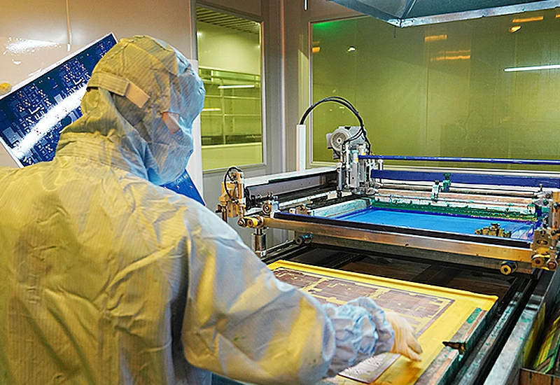
Coating, Exposure and Development on Both Sides of The Circuit Board
Visual Appearance of Solder Mask
The appearance of the solder mask is important but not the only criterion for judging quality. Green is the industry standard, but red, blue, black, white, and yellow are widely used for applications such as medical PCB board fabrications, consumer electronics, and high-end customization.
Color differences may appear due to coating thickness, curing temperature, or copper reflectivity. These minor differences do not affect performance or soldering quality. According to IPC-A-600, acceptable variations include small scratches, bubbles, or rework marks, as long as functional requirements are not compromised.
Relationship Between Component Holes and Solder Mask
In PCB design, the relationship between plated through-holes (PTH) and solder mask strongly affects manufacturability and soldering reliability.
-
For THT components, hole walls must remain free of solder mask to ensure full solder wetting.
-
For microvias or vias under 0.45mm, solder mask thickness and ink fluidity may cause partial residue in holes.
-
When the aperture is less than 0.3mm, solder mask may even fully block the via. This is not a defect but a process-related phenomenon.
Edge Coverage and Solder Mask Retreat Distance
The solder mask should fully cover copper foil but reserve a 0.1–0.15mm retreat distance from pads to avoid covering them. This detail is especially critical for high-frequency PCBs, HDI PCB boards, or BGA packages, where solder mask thickness control directly impacts pad alignment and solderability.
Requirements for Solder Mask Coating Under Different PCB Structures
The solder mask layer is usually applied to both sides of the circuit board in the printed circuit board assembly to form a standard double-sided solder mask structure, which is the most common design form and is suitable for most double-sided circuit boards. In this configuration, both the front and back sides need to be coated, exposed and developed to protect the copper wires, pads and isolate external contaminants.
However, for multilayer PCB and high-density interconnect boards (HDI PCB) with more complex structures, the requirements for solder mask coating are also more refined. This type of PCB usually contains a large number of micro blind holes, laser drilling and dense wiring areas. Local thickening or multiple coating processes may be used in the manufacturing process to enhance the protection of key circuit areas and improve welding reliability and durability.
In addition, in some high-frequency or high-voltage applications, in order to improve the insulation performance of the solder mask layer, customized protection may also be achieved by adjusting the thickness or using special materials (such as ceramic solder mask). Therefore, the number of solder mask layers depends not only on the board structure, but also on the comprehensive influence of electrical performance, packaging density and terminal application requirements.
Available Coating Processes
Solder mask can be applied by using the following methods:
- Curtain Coating: Applicable to large-volume boards, uniform thickness
- Inkjet spraying: Suitable for high-precision, low-volume products
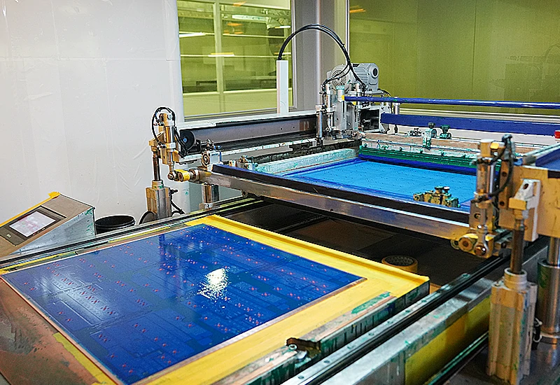
- Screen printing: Suitable for simple graphics, low-cost applications
- LPI (liquid photoresist): The most commonly used technology, exposure and development after photosensitization
Exposure Process of Solder Mask
The solder mask is developed through a graphic exposure process to ensure that the solder mask pattern is accurately aligned with the pad. The UV exposure equipment uses a mask to align the PCB, and cleans the unexposed area after ultraviolet exposure to form a solder mask opening. Common methods include:
- Manual Film Exposure: Easy to operate, suitable for small-batch PCB boards production
- Semi-Automated Film Exposure: Improve accuracy and efficiency through mechanical alignment
- Fully Automated Film Exposure: With precise alignment and stability, it is suitable for high-precision production of large-scale printed circuit manufacturing
- Manual Direct Imaging (Laser/LED): Direct exposure without film, manual material processing. Suitable for HDI, finer structures and smaller batches
- Automated Direct Imaging (Laser/LED): Direct imaging does not require film, and directly uses laser or LED light sources to accurately draw graphics. It is particularly suitable for HDI PCB and fast proofing projects, greatly improving resolution and graphic consistency

Classification of Solder Mask Materials
Common solder mask materials are divided into:
● Thermal Curing Type
This type of material needs to be cured at high temperature, has excellent heat resistance and adhesion, and is suitable for demanding high-reliability applications such as multi-layer rigid boards, ceramic PCBs or military and automotive control modules. Its excellent insulation and chemical corrosion resistance make it the first choice for high-frequency and high-power applications.
● UV Curing Type
Rapidly cured with ultraviolet light, suitable for single layer circuit board, large-volume consumer electronic boards such as TVs, power boards, etc. This type of material has high production efficiency and low cost, and is widely used in the field of mid- and low-end electronic products.
● Hot Melt Type
The lowest cost and simple process, but poor heat resistance and mechanical properties. Generally used in simple Aluminum PCBs or low-end lighting products, not suitable for complex or high-temperature working environments.
Acceptance Criteria and Quality Standards for Solder Mask
According to IPC-6012, IPC-A-600, and IPC-SM-840, the criteria include:
-
No cracks or peeling
-
Clear solder mask edges without oil diffusion
-
No pinholes or thickness irregularities
-
Solder mask thickness between 10–30 μm
-
Appearance compliance: matte, semi-matte, or glossy finish
Note on solder mask thickness: Proper thickness ensures balance between solder protection, insulation, and solderability. If too thin, the solder mask may crack or fail to insulate; if too thick, it may cover pads or affect hole integrity.
Matt or Glossy Green Solder Mask Varnish
Depending on the process, the surface of green solder mask can be matte, semi-matte or glossy. Matte is suitable for industrial control PCBs to reduce light reflection, while glossy has better visual effect and is often used in consumer electronic appearance boards. If you or your customers prefer to use conformal coating, or your end customers have requirements for appearance, please contact us.
Through-hole Residue and Solder Mask Contamination
If through-holes are not cleaned thoroughly after soldering, flux or oxide residues may contaminate the solder mask, causing blistering, peeling, or subsequent reliability reduction, so cleaning and baking treatments need to be strengthened.
Solder mask residues in through-holes are mainly caused by 3 factors:
● Through-hole aperture is too small
When the final aperture of the through-hole is less than Ø0.45 mm, especially less than Ø0.3 mm, the solder mask ink is difficult to completely remove during deposition or exposure and development, and it is easy to form residues on the hole wall or inside the hole, or even completely block the hole. This is because the ratio between the surface tension of the ink and the aperture is too large, resulting in incomplete cleaning.
● Too thick solder mask coating
If the thickness of the solder mask is not properly controlled during printing or spraying, especially on high-density boards, the amount of one-time coating is large, which is easy to cause ink to accumulate at the hole mouth. When the subsequent development and rinsing steps fail to completely remove the excess material in the hole, it will cause residues.
● Insufficient development and rinsing process
If the exposure energy of the solder mask is insufficient, the development time is too short, the water pressure is insufficient, or the nozzle angle is not good, the ink in the through hole may not be fully developed and discharged, and the residue will be difficult to remove after solidification. This problem is more likely to occur when the parameters of the automated processing equipment are not matched.
A Few Things You Need to Know About Solder Mask
Solder mask is not an insulating material and cannot completely replace the insulating layer design
The thickness of solder mask in high-frequency PCB will affect signal transmission and impedance
Black solder mask is not easy to detect, so it is recommended to use it with caution in industrial products
Some high-temperature applications require white ceramic solder mask materials
As an indispensable part of PCB manufacturing, the design and processing quality of solder mask directly affect the weldability, electrical performance and appearance quality of the finished product. Whether in consumer electronics or aerospace, automobile, or medical equipment, a reasonable solder mask process is the guarantee of high-reliability PCB. Choosing SCSPCBA printed circuit board manufacturers, the right materials, standards, and processes are the important cornerstones to help you move towards high quality.
Why Solder Mask Thickness Matters in Circuit Board Manufacturing Quality
Solder masks’ design, thickness, and process quality directly impact solderability, reliability, and electrical performance. Correct solder mask thickness control ensures long-term durability and high-yield PCB manufacturing, from consumer electronics to automotive, aerospace, and medical applications.
At SCSPCBA, we follow IPC standards to guarantee that solder mask thickness, materials, and coating processes meet the highest requirements for one-stop PCB and PCB assembly manufacturing.
Search
Latest News
 SCSPCBA MES System: A Unified Manufacturing Execution Platform for PCB & PCBAJanuary 5, 2026 - 1:00 am
 Best Wishes for the New Year 2026: Manufacturing Support Continues Without InterruptionDecember 30, 2025 - 1:00 am
 Box Build Quote Service: A Practical One-Stop PCBA Solution for OEM & ODMDecember 30, 2025 - 1:00 am
 What Engineers and Buyers Should Know About Automotive PCB AssemblyDecember 25, 2025 - 1:00 am
 A Data-Driven Approach to BOM Management and Smart BOM Quoting in PCB AssemblyDecember 20, 2025 - 1:00 am

