Circuit Board Design And Manufacturing
PCBA panel plays a vital role in the field of electronic manufacturing. It refers to splicing multiple printed circuit board assemblies into a large board so that multiple circuit boards can be processed and soldered simultaneously during production. Printed circuit board design can improve production efficiency, reduce costs, optimize PCB board production processes, etc., providing a solid guarantee for the manufacture of electronic products.
1. Printed Circuit Board Design
Paneling is the process of processing and welding multiple circuit boards in the same period through printed circuit manufacturing equipment during the design printed circuit board process.
It greatly improves production efficiency, effectively reduces production costs, reduces the possibility of human errors, and can further improve the efficiency and quality of PCB assembly manufacturing.
2. PCB Circuit Board Design Principles
When designing circuit board, multiple factors must be considered to ensure that materials can be used as effectively as possible during the printed circuit assembly process, reduce PCB material waste, and improve PCB board production efficiency and product quality.
● Uniform Circuit Board Size and Shape
The size and shape of the circuit board should be as consistent as possible, ensuring that there is enough clearance between each single PCB board, and adding positioning holes and reference marks on the panel to reduce the complexity and difficulty of the circuit board manufacturing process.
For larger PCB board fabrication, PCB manufacturing and assembly need to undergo reflow soldering or wave soldering and have a width of ≥60mm, the number of panels in the direction perpendicular to the conveying edge should generally not exceed 2 rows.
For smaller PCB manufacturing, if the circuit on board size is very small, the number of panels in the direction perpendicular to the conveying edge can exceed 2 rows, but the total width in the direction perpendicular to the conveying edge cannot exceed 150mm, and tooling must be used during production to prevent PCBA circuit board deformation.
● Printed Circuit Board Double-sided V-grooves
Design V-grooves between circuit card assembly, and open V-grooves between boards, making the connection the weakest area of the single board, and separating the panels by hand or machine.
● Choose The Right Circuit Board Paneling Method
With a size of 80~125mm, the circuit board uses the same direction paneling design
Centrosymmetric printed circuit board paneling is often used to produce multiple circuit boards with the same shape and similar layout. The PCB printed circuit board are arranged horizontally, vertically or obliquely symmetrically with the center point as the symmetry axis. If there is a large hair shape produced by the paneling, an auxiliary block can be added in the middle of the panel.
For gold finger circuit board that require central symmetric paneling, the production of the gold finger board is relatively special. The gold finger part needs to be gold-plated, and each finger needs to lead out copper wire to increase conductivity. Therefore, the paneling needs to be paid attention to the gold finger needs to be exposed outside the board to facilitate the final electroplating.
Mirror symmetric paneling, the front and back of the circuit board are completely consistent after paneling. Double-sided printed circuit board are all smd components, which can use a steel mesh to reduce the preparation time and meet the conditions of reflow soldering.
● Reinforced Circuit PCB Frame
Adding a reinforced frame around the printed circuit board panel can improve the rigidity, especially in large-size printed circuit card panels. Adding support points can ensure the flatness of the single circuit card during electronic assembly.
● Optimize Circuit Board Manufacturing Process
Take the processing of gold finger circuit board as an example. In the panel PCB board design, the processing order of gold fingers should be considered. The gold finger area should avoid wiring and electronic component placement, and a protective layer should be added to prevent damage during processing. These printer PCB design principles help to achieve an efficient and low-cost pcb board fabrication process while meeting strict printed circuit board manufacturing process and quality requirements.

3. Printed Circuit Assembly Panelization Case
In PCB board production, the mismatch between circuit board component selection and circuit design may lead to a series of production and quality problems. The following is a detailed case analysis, problem analysis, and solution.
● Printed Circuit Assembly Case Description
During the printed circuit manufacturing process, some electronics components were offset or could not be properly welded after welding. The circuit design caused the components to be unable to be installed or work properly. Due to the mismatch, welding defects occurred, affecting the quality of the circuit board.
● PCB Fabrication and Assembly Problem Analysis
Wrong or inaccurate components are used, resulting in incorrect placement of PCB board parts; or during soldering, the pad size or spacing does not match the electronic parts pins, resulting in loose soldering or short circuit.
● PCB and Assembly Solution
After the PCB circuit board design is completed, a strict design review is carried out, including checking the circuit board size, electronic components type, circuit design, heat dissipation design, etc.
During the printed circuit manufacturing process, functional testing is performed to ensure that the circuit board reduces operational errors and mistakes and ensures circuit assembly quality.
Latest News
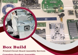
 Box Build Printed Circuit Board Assembly Services | Complete Product AssemblyFebruary 25, 2026 - 1:00 am
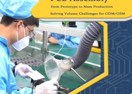
 PCB Assembly from Prototype to Mass Production: Solving Volume Challenges for ODM/OEMFebruary 10, 2026 - 1:00 am
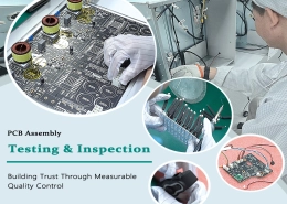
 PCB Assembly Testing & Inspection: Building Trust Through Measurable Quality ControlFebruary 5, 2026 - 1:00 am
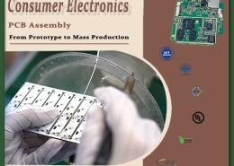
 From Prototype to Mass Production: Consumer Electronics PCB AssemblyJanuary 30, 2026 - 1:00 am
 Industrial Control PCBA Solutions With Strict DFM and MES ControlJanuary 25, 2026 - 1:00 am