Efficient Soldering: A Critical Role in Printed Circuit Board Manufacturing
1. PCB Design
PCB design is a crucial part of electronic product development. A good PCB board design ensures the printed circuit’s functionality and improves overall performance and reliability. During the design process, engineers need to consider a variety of factors, including selecting the right PCB material (such as FR-4, Carbon Ink PCB, Impedance Controlled PCB, etc.), component layout, determining solder materials (such as lead-free solder alloys), flux, signal integrity, power management, etc. Reasonable circuit board layout and component placement can reduce signal interference and improve circuit stability.
After completing the basic circuit board design, the next step is to select the production process. Wave soldering is a commonly used soldering method suitable for mass production. Wave soldering heats the solder to a liquid state to form a soldering wave. The solder can effectively combine with the component pins and pads when the circuit board passes through the wave. This process not only improves soldering efficiency, but also ensures the quality and consistency of solder joints.
2. Preliminary Preparation of Wave Soldering Machine
- Check whether the ventilation equipment of the wave soldering machine is in good condition;
- Check whether the timing switch of the wave soldering machine is in good condition;
- Adjust the tin bath temperature indicator up and down, and use a thermometer to measure the temperature 10-15 mm below the tin bath liquid surface to determine whether the temperature changes with it;
- Turn on the preheater switch and check whether it heats up and whether the temperature is normal;
- Adjust the height of the blade according to the thickness of the circuit PCB and the length of the component leads, then tighten the blade holder and make it stable, turn on the machine and visually check the rotation of the blade, and finally check whether the safety device fails;
- Check the compressed air supply in the flux container: Pour the flux, adjust the air inlet valve, and start the machine to allow the flux to foam. Use a sample printed board to adjust the foam to 1/2 of the board thickness, and then tighten the intraocular pressure valve. When the formal operation is completed, do not move this valve, and only open the air inlet switch;
- After all the above procedures are normal, the various required process parameters can be preset to the relevant positions of the equipment.
3. Wave Soldering – Flux Adding Area
It consists of an infrared sensor and a nozzle. The infrared sensor is used to monitor the entry of the PCB circuit board. If there is a sensor, the width of the circuit board will be measured. The flux is used to remove oxides on the welding surface, reduce surface tension, promote good solder wetting with the circuit on board and component pins, and form a protective film on the welding surface of the board for circuit. The flux is usually added to the PCB circuit board by spraying or immersion before welding to ensure the effectiveness of welding.
Different types of flux (such as water-soluble, no-clean, resin type, etc.) are suitable for different welding requirements and circuit board materials. Choosing the right flux can improve the welding quality.
4. Wave Soldering – Preheating Zone
The PCB passes through the preheating zone and gradually heats up, so that the temperature of the entire circuit board is uniform to reduce thermal shock and improve welding quality. The preheating temperature directly affects the welding quality and the reliability of components. The preheating temperature should be set within a suitable range to ensure that the electronic components and pads on the PCB board reach a certain temperature before welding, remove moisture from the circuit board and components, reduce the risk of bubbles and poor solder joints during welding, and facilitate the rapid melting and wetting of the solder.
The specific setting value of the preheating temperature is adjusted according to factors such as the material, thickness and component type of the PCB circuit board to alleviate the thermal stress generated during the welding process, reduce the risk of thermal damage to the circuit board and components, and refer to the actual performance of the wave soldering machine.
5. Wave Soldering – Cooling Stage
The circuit board passes through the cooling zone, and the solder solidifies to form a solid solder joint. The proper cooling rate is critical to the quality of the solder joint. Too fast cooling may cause solder joint embrittlement, cracks or poor soldering, while too slow cooling may cause the solder joint to fail to fully solidify, affecting the contact resistance. During the cooling process, the solder joint’s thermal stress and surrounding materials must be controlled to reduce thermal deformation and damage. After cooling, the appearance and quality of the solder joint need to be checked to ensure that the solder has not deteriorated or adhered during the cooling process.
6. Cleaning The Printed Circuit Card
After soldering, flux, solder and other contaminants may remain on the electronic circuit board, affecting performance. Therefore, the parts of printed circuit board residues should be cleaned to ensure the quality of soldering and the reliability of electronic components, ensuring that they are not damaged and meet the quality standards. Common cleaning methods include ultrasonic cleaning, spray cleaning and immersion cleaning. After cleaning, the PCBA board must be thoroughly dried to prevent residual moisture from affecting subsequent assembly and performance. Hot air drying or vacuum drying methods are usually used.
7. Final Assembly
The wave-soldered circuit PCB board is attached to the product housing or base, usually using screws, snaps or adhesives to ensure a firm and reliable connection to form a complete product.
After PCB board assembly, functional testing is performed to ensure that all components work properly, including power supply, signal transmission and user interface response. After all functional tests pass, the housing is encapsulated and sealed to protect the internal components from the external environment.
 An Engineering Perspective: How AI Hardware Challenges PCBA – and How We RespondJune 29, 2026 - 9:54 am
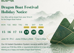
- Dragon Boat Festival Holiday Notice 2026June 18, 2026 - 8:47 am
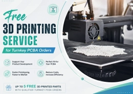
- Free 3D Printing Service for Turnkey PCBA OrdersJune 3, 2026 - 10:28 am
- Your PCBA Projects Keep Moving Forward During the Labor Day HolidayApril 27, 2026 - 10:17 am
- AI Hardware PCBA: The Problems You Only Discover After Production StartsApril 24, 2026 - 10:17 am