Consumer Electronics PCB Manufacturing Assembly for Modern Devices
PCB assembly accurately welds micro-components such as resistors, capacitors, integrated circuits (ICs), and connectors onto the PCB board to form a complete circuit. Without high-quality assembly, no matter how advanced the circuit design is, it cannot realize basic functions such as signal transmission, power management, and data processing, which are the basis for the operation of consumer electronics products (such as mobile phones, headphones, and smart watches). From wearable devices and smart home controllers to audio equipment and portable electronics, consumer electronics PCB manufacturing requires a highly flexible and data-driven approach to electronic assembly services.
The manufacturing of consumer electronics printed circuit board assembly is characterized by high integration, precision and automation to meet the stringent requirements of modern electronic products for miniaturization, high performance and high reliability.
1. Manufacturing Characteristics of Consumer Electronics PCBA
(1) Highly Automated Production
The manufacturing of consumer electronics PCBA is highly dependent on automated equipment
SMT Placement Technology
Surface mount technology (SMT) is the core process, using high-precision placement machines to quickly and accurately place micro surface mount components (SMC/SMD) on PCB pads. Modern placement machines use dual-beam systems and visual alignment technology to improve speed and accuracy, especially for dense BGA (ball grid array) components in mobile phones, tablets and other products.
DIP Plug-in Technology
For components that are large, high-power or require high mechanical strength (such as connectors, transformers), through-hole technology (THT) is still used for plug-in, usually in combination with the SMT process.
(2) Precision Manufacturing and High-density Integration
In pursuit of thinner and lighter designs, PCBA is developing in the direction of high-density interconnection (HDI).
- Fine lines and micro holes
Laser drilling technology is used to create tiny blind holes and buried holes, significantly improving wiring density. - Multilayer board structure
Multi-layer PCBs (such as 6-16 layers or even higher) are widely used to accommodate more circuits and components while optimizing signal integrity. - Advanced Substrate
Use high-performance glass fiber substrates such as FR-4, and high-temperature resistant materials (such as Tg170) to meet the heat dissipation challenges caused by high integration.
(3) Strict Quality Inspection and Testing
With dense circuit boards and components and numerous solder joints (tens of thousands), quality control is critical.
- AOI Inspection
The automatic optical inspection system performs high-speed, high-precision visual inspection of component position and solder joint quality after SMT and reflow soldering. - X-ray inspection
For invisible solder joints such as BGA, X-ray layered imaging technology is used for non-destructive inspection. - Functional Testing
Conduct ICT (in-circuit testing) and functional testing before final assembly to ensure that the board fully meets the design specifications.
(4) Advanced Surface Treatment Process
To ensure good solderability and long-term reliability, the circuit board surface will undergo special treatment.
- Electroless nickel/gold plating (ENIG)
Forming a uniform nickel/gold layer on the surface of copper foil with good oxidation resistance, it is a mainstream process for consumer electronics. - Other processes
OSP (organic soldering film), immersion silver, immersion tin and other processes may also be used, selected based on cost and performance requirements

2. Fast Prototyping vs Mass Production PCB Assembly
In the consumer electronics PCBA field, choosing between rapid prototyping and mass production PCBA assembly depends not only on production volume but also impacts time to market, cost control, and product iteration speed.
Thanks to its flexible manufacturing system, SCSPCBA can support both production stages simultaneously within the same integrated consumer electronics PCB fabrication and assembly.
(1) Consumer Electronics Fast Prototype PCB Assembly
Fast-prototype PCB assembly manufacturing focuses on engineering verification and functional validation before scaling. It is commonly used for consumer electronics products such as wearables, smart home devices, and IoT modules.
☆ SCSPCBA Prototype Configuration
To support rapid iteration, SCSPCBA operates a dedicated sample SMT line, optimized specifically for prototype builds. In addition, a combination of manual and semi-automatic placement enables greater flexibility when handling high-mix, low-volume orders.
Meanwhile, engineering-assisted DFM reviews are integrated early in the process to identify manufacturability risks before scaling.
☆ Typical Prototype Capabilities
Prototype PCBA orders can be completed within 24–72 hours, depending on board complexity and material availability.
Typically, order volumes range from 1 to 50 boards, while flexible BOM substitution helps mitigate component shortages.
At the same time, a fast design feedback loop allows engineers to refine layouts and component choices efficiently.
☆ This Setup is Ideal for
- Hardware startups
- New consumer electronics models
- Rapid design iteration projects
(2) Mass Production PCB Assembly for Consumer Electronics
Once a design is validated, consumer electronics require stable, repeatable, and scalable printed circuit manufacturing to meet market demand.
☆ SCSPCBA Mass Production SMT Resources
To meet these requirements, SCSPCBA operates five SMT lines in total, including three standard SMT lines (1+1 configuration) dedicated specifically to consumer electronics production.
As a result, the total SMT placement capacity reaches 40,000,000 placements per day, supported by inline SPI and AOI inspection.
Furthermore, MES-driven process control ensures real-time monitoring and consistent quality across large production runs.
☆ DIP & Through-Hole Support for Large Volumes
In addition to SMT capabilities, SCSPCBA provides two wave soldering lines designed for high-volume consumer electronics products.
With a DIP capacity of 350,000 placements per day, these lines efficiently handle through-hole components.
For mixed-technology boards, manual soldering lines are also available to support complex or selective assembly requirements.
☆ This Configuration Supports
- High-volume consumer circuit board manufacturing
- Stable yield across large batches
- Cost optimization through SMT line balancing
(3) Consumer Electronics PCBA Capability Comparison Table
| Item | Fast Prototype PCB Assembly | Mass Production PCB Assembly |
|---|---|---|
| Typical Volume | 1–50 pcs | 1,000–100,000+ pcs |
| SMT Line Type | Sample SMT Line | Standard SMT Lines (3) |
| Focus | Speed & validation | Cost & consistency |
| Lead Time | 24–72 hrs | 5–15 days |
| DFM Depth | Engineering review | Full process optimization |
| Automation Level | Semi-auto | Fully automated |
| Welding Type | Manual welding | Wave soldering |
(4) Why One Manufacturer for Both Stages Matters
Using the same electronics assembly services provider for both prototyping and mass production offers clear advantages:
- Consistent DFM rules
- BOM continuity
- printed circuit board manufacturing process inheritance
- Faster ramp-up with fewer surprises
With MES system tracking, all process data from prototype builds can be reused during volume production, reducing yield loss during scaling.
(5) From Idea to Market—Quote in Seconds
Whether it is smart wearable brands、IoT and smart home device companies、audio & video electronics manufacturers or consumer electronics startups and ODMs, you can all benefit from our AI-powered online quotation system
To support both fast prototyping and mass production, SCSPCBA provides an online PCBA quotation platform that allows users to:
- Upload Gerber & BOM
- Get instant price feedback
- Compare prototype vs mass production costs
- Identify DFM risks early
3. Advantages of High-Speed SMT Production Lines in the Consumer Electronics Field
(1) High Production Efficiency
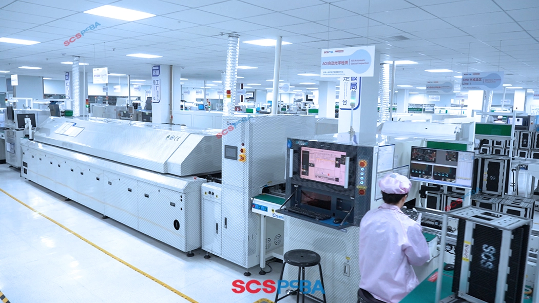
- Placement speed: 100,000-150,000 components/hour
- Fully automated SMT equipment can place tens of thousands of electronic components per hour, an efficiency increase of more than a hundred times compared to traditional manual insertion, enabling rapid response to the large-scale, fast-paced production demands of consumer electronics products.
(2) High Placement Accuracy
- Placement accuracy: ±0.025 mm
- Equipped with high-precision vision systems and motion control systems, it can achieve precise positioning of miniature components (e.g., 01005 size, 0.4mm × 0.2mm), effectively reducing placement errors and significantly improving circuit board yield and reliability.
(3) Supports Miniaturization and High-Density Integration
Precise SMT (Surface Mount Technology) placement ensures accurate alignment of components and pads, avoiding problems such as false soldering and short circuits. SMT technology is key to achieving the lightweight design and functional integration of consumer electronics products such as smartphones, tablets, and wearable devices. It can place components with extremely small spacing (e.g., 0.3mm), meeting the ever-evolving compact design needs of products.
(4) Reduced Overall Costs
Consumer electronics products demand large-scale, low-cost manufacturing. Automated SMT production lines for PCB board assembly achieve high-speed, high-precision component placement, significantly replacing manual operations and dramatically increasing production efficiency. In addition, by optimizing panel design (e.g., combining multiple small boards into one), substrate utilization is maximized, reducing changeover time and thus lowering the unit product cost.
(5) Flexible Production Adaptability
Modern high-speed SMT production lines adopt a modular design, enabling quick changeovers and adapting to the rapid iteration, small-batch, and customized production trends in consumer electronics.
4. Online Quotation System for Consumer Electronics PCB Assembly
Due to the inherent characteristics of the circuit board industry, quoting is not only complex but also highly specialized. This results in high labor costs and significant quoting errors. SCSPCBA’s intelligent online quotation system allows users to select dimensions, board materials, and manufacturing processes, automatically calculating the price.
(1) 24-hour self-service quoting and ordering improves the quality of PCB assembly services.
(2) Professional and flexible quoting for consumer electronics PCBA reduces pre-sales costs.
(3) Large discount coupons available, enjoy discounts on PCB and PCBA orders, free stencils, the more you order, the more you save.
(4) Automatically analyzes Gerber files and Bill of Materials (BOM).
(5) Detects Design for Manufacturability (DFM) risks.
(6) MES system: Utilizes barcode technology to scan production orders and upload progress data in real time, allowing customers to stay informed about the production progress of their consumer electronics PCBA manufacturing orders, guaranteeing on-time delivery;
(7) 7×12 hour attentive service
(8) Ordering process: Customer registration → Login → Automatic quotation → Upload documents → Place order → Progress inquiry → Receipt confirmation
5. DFM Support for Consumer Electronics PCBA
In the early stages of circuit design, integrating the process requirements, equipment characteristics, quality standards, and cost control logic of consumer electronics PCBA manufacturing into the design plan is crucial. DFM (Design for Manufacturability) not only ensures functionality but also enables efficient mass production, stable reliability, and controllable costs.
For example, a customer-designed PCB board might meet electrical performance requirements but neglect the precision requirements of high-speed SMT assembly lines; the selected PCB board components might meet functional specifications but be difficult to adapt to automated welding processes. DFM can identify and optimize these issues in advance, ensuring a seamless connection between the design plan and the PCB fabrication manufacturer’s production capabilities.
As a printed circuit board assembly manufacturer directly involved in production, SCSPCBA has witnessed numerous regrettable situations caused by neglecting DFM (Design for Manufacturability). DFM primarily focuses on the following aspects:
(1) Avoiding Design-Production Disconnect and Reducing Unnecessary Costs
Many customers’ designs work perfectly in the laboratory, but are incompatible with mass production: for example
- Using too many blind/buried vias on the PCB board directly increases processing costs by 15%-30%;
- The PCB board parts layout is too dense to be recognized by the manufacturer’s AOI (Automated Optical Inspection) equipment, requiring manual inspection, which drastically reduces efficiency.
These problems are difficult for customers to anticipate, but through DFM, the manufacturer can adapt to the printed circuit board manufacturing process in advance, avoiding ineffective manufacturing caused by designs that meet specifications but are difficult to mass-produce.
(2) Shorten Mass Production Cycles and Seize Market Opportunities.
DFM (Design for Manufacturability) can prevent over 90% of manufacturing risks in advance, allowing the first trial production yield to exceed 99%. SCSPCBA’s collaborating ODM/OEM customers, after DFM optimization, have seen an average reduction of 30% in development cycles, enabling small to medium-scale production within 1-2 weeks after design finalization.
(3) Improving the Performance of Consumer Electronics PCB Assemblies
- EMI interference caused by unreasonable wiring
Performance degradation caused by improper heat dissipation layout
Batch variations caused by solder pad design defects
… …
These problems in the PCB design phase, once they enter the PCB production process, can pose risks such as substandard performance.
DFM (Design for Manufacturability) can optimize the design from the source, for example, by improving signal stability through EMI control and ensuring continuous operating performance through thermal design, while also mitigating risks in advance, making consumer electronics PCBA performance more stable and the production process more controllable.
6. Core Problems Solved by MES in Consumer Electronics PCBA Manufacturing
Common problems in consumer electronics orders include: multiple SKUs, small batches, and frequent order changes; simultaneous production of samples and mass production; and significant differences in cycle times for SMT, DIP, and assembly testing.
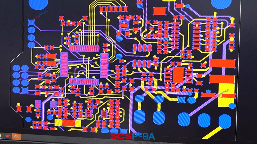
In high-density consumer electronics PCBA assembly, issues such as SMT placement parameters and variations in manual soldering operations occur, but are difficult to quickly pinpoint.
More and more consumer electronics customers require complete production records, traceable to batch, process, and time point.
To address these issues, SCSPCBA’s MES is adapted to the manufacturing requirements of consumer electronics PCBAs.
(1) SCSPCBA Focuses on The Following in MES Implementation
- Does it have mature, standardized modules?
- Does it support low-code or parameterized configuration?
- Can it generate actual production value within 3-6 months?
(2) MES Collects the Following Data in Real Time
- Work order status
- Equipment load
- Process progress
This significantly reduces the risks associated with repeated plan adjustments
(3) MES Enables Traceability
Key process parameters, test results, and operation records for each board are linked, so that anomalies are no longer limited to the result level, but can be traced back to each specific circuit board manufacturing process step.
(4) HDI Consumer Electronics Manufacturing
When handling urgent orders for 6-layer HDI consumer electronics PCBs, MES supports:
- Work-in-process quantity management at the process level
- Parameter linkage across different process segments
- Rapid switching and continuity of process records
7. Consumer Electronics PCBA FAQ
How is consumer electronics PCBA different from industrial or automotive PCBA?
Consumer electronics PCBA typically features:
- Shorter product life cycles
- Faster iteration
- Higher volume but lower per-unit cost
- Greater emphasis on speed and scalability rather than extreme reliability standards
What types of consumer electronics products require PCB fabrication and assembly?
Common applications include:
- Smart wearables
- Smart home devices
- Audio and video equipment
- IoT consumer modules
- Portable electronics and accessories
What PCB technologies are commonly used in consumer electronics?
Typical PCB specifications include:
- 2–6 layers
- HDI structures
- Fine-pitch components (≤0.4 mm)
- BGA, QFN, LGA packages
What SMT capabilities are important for consumer electronics PCB manufacturing and assembly?
Key SMT requirements include:
- High placement speed
- Support for 0201 / 01005 components
- High placement accuracy (±0.025 mm)
- Stable performance in high-mix production
What role does DFM play in consumer electronics box build assembly?
DFM (Design for Manufacturability) helps:
- Reduce assembly defects
- Improve yield stability
- Lower rework and material waste
- Optimize cost before mass production
- Early DFM is especially important for dense consumer electronics designs.
What testing methods are commonly used in consumer electronics PCBA?
Typical testing includes:
- AOI (Automated Optical Inspection)
- SPI (Solder Paste Inspection)
- Functional testing
- Power-on and basic reliability tests
- Testing depth depends on product complexity and risk tolerance.
How is cost controlled in high-volume consumer electronics printed circuit manufacturing?
Cost control methods include:
- High-speed SMT automation
- BOM optimization
- Panelization optimization
- Yield improvement through process control
- Mass production efficiency is a key cost driver.
What order volumes are suitable for consumer electronics circuit board manufacturing?
Consumer electronics PCBA typically covers:
- Prototypes: 1–50 pcs
- Small batch: 100–1,000 pcs
- Mass production: 10,000 pcs and above
- Flexible manufacturers can support all stages.
How does an online PCBA quotation system help customers?
Online quotation systems allow customers to:
Upload Gerber and BOM files
Receive pricing in seconds
Compare prototype vs mass production costs
Identify DFM risks early
This significantly shortens decision-making time.
How do I choose the right consumer electronics printed circuit board assembly manufacturer?
Key selection criteria include:
- Proven SMT and assembly capacity
- Experience with consumer electronics products
- Strong DFM and quality systems
- Transparent pricing and fast quotation
- Ability to scale from prototype to mass production

