How to save PCBA manufacturing costs to the maximum extent? A customer’s printed circuit board optimization story
When Noemi first contacted SCSPCBA, he was in the early stages of his business, with only a preliminarily completed prototype of a health smartwatch and a long list of imaginative features: heart rate monitoring, blood oxygen tracking, sleep analysis, and fall reminders for the elderly… These features all rely on precise electronic design and stable manufacturing support. However, he knew very well that printed circuit boards and subsequent PCBA manufacturing were the most expensive parts of health AI hardware. Once costs get out of control, mass production plans will fall through. But he also understood that if the design is optimized from the source, the selection is reasonable, the mounting is streamlined, the testing process is standardized, and the PCB board production cost is controlled, this device will have the opportunity to enter thousands of households truly. Noemi is not the only hardware entrepreneur with this problem, and SCSPCBA is the “money-saving key” he found.
Step 1: Save money from PCB design
The first generation prototype drawings brought by Noemi were fully functional but had messy wiring, complex board layers, and serious redundant interface stacking. After the first round of evaluation, the engineering team of SCSPCBA decided to reconstruct the entire circuit architecture, starting from optimizing printed circuit board design. SCSPCBA streamlined the original 6-layer PCB board to 4 layers, while compressing the routing length and removing unenabled communication interfaces (such as redundant UART and spare BLE module interfaces). This step directly saved more than 20% of the pcb board fabrication cost and the subsequent mounting difficulty of health wearable devices.
While reorganizing the stacking structure of the circuit board, the wiring symmetry and ground layer distribution of key chips were optimized, and the signal integrity and electromagnetic compatibility performance were improved. For Noemi, this means not only saving money, but also ensuring the long-term stable operation of health smart watches in the medical and health field.
Step 2: Component optimization plan, optimize 30% of space saving from BOM
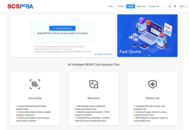
PCB board assembly cost-saving techniques are often hidden in the BOM list. Noemi’s original BOM contained multiple imported brand chips, with high unit prices and unstable delivery dates. After evaluation, SCSPCBA’s procurement team proposed suggestions for replacing chips to reduce the manufacturing cost of circuit boards. On the premise of ensuring that the function, compatibility and quality are not affected, more than ten models including power management ICs, logic chips, and some sensor modules were replaced.
For example, the original TI power chip cost more than US$2 per chip. After replacing it with a domestic high-cost-effective brand, the cost dropped to US$0.78 per chip, and the supply cycle was more stable. After evaluating the compatibility of the pcb board layout, we also helped Noemi adjust the pad package so that the replacement components can seamlessly match the original design.
In the end, the cost of the entire set of electronics components was reduced by an average of about 30%. This not only gave Noemi’s production budget some breathing room, but also greatly reduced the risk caused by chip price increases or shortages.
Step 3: SMT patch cost control strategy
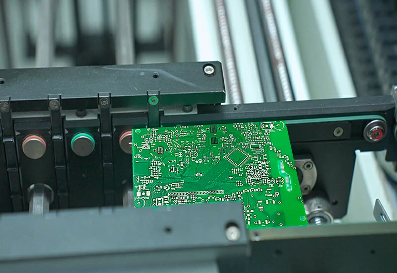
After the PCB circuit board design is finalized, the next key link is the optimization of the SMT surface mount process. Noemi’s original design contains multiple specially-shaped components and non-standard packaged devices, which not only increases the difficulty of programming the surface mount device, but also increases the SMT working hours and surface mount electronic components defect rate.
SMT process engineers adopt a series of circuit board panel patch optimization techniques:
- Use standard surface mount components (0603/0402) to improve the patch speed
- Optimize the uniformity of patch direction, centralized component arrangement and PCB panel method from scratch
- In terms of patch pad design, fine-tune the pad size of some components to make it more compatible with the placement equipment identification mechanism and reduce offset soldering and cold soldering problems.
- In the batch PCB board production stage, use a multi-joint pcb panelization structure to mount multiple circuit boards at one time and reduce machine line change time
- By optimizing the patch process parameters and using high-precision steel mesh, ensure uniform solder thickness and improve welding yield
- The patch efficiency of the entire SMT line has increased by 22%, and the surface mount electronics cost has decreased by 15%
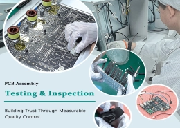
Step 4: PCBA functional test: modular testing allows each board to pass 99.8%
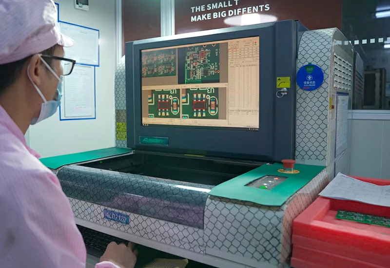
In medical and health hardware, the reliability of PCB manufacturing and assembly is directly related to the user’s life safety, so Noemi is very cautious in the PCBA testing stage. The initial plan was to manually test each board, but SCSPCBA recommended the use of modular functional test fixtures to replace manual labor, a one-time investment, and long-term savings.
SCSPCBA designed a dedicated FCT test fixture for Noemi, and divided the core functional modules such as heart rate, blood oxygen, vibration, battery charging and discharging into independent test channels, and realized automatic testing and recording after inserting the fixture. Compared with the manual test of 5 minutes for 1 circuit board, the automatic test platform only takes 30 seconds to complete the entire process.
At the same time, for the electrical test part of the printed circuit board, we introduced the ICT (in-circuit test) process to 100% check for problems such as solder joint short circuit, power supply abnormality, and voltage offset. The printed circuit board testing pass rate has increased from the original 94.2% to 99.8%.
Noemi exclaimed: “The average testing cost per board for circuit has dropped from ¥5 to ¥1.6. This is the first time I have seen that pcb board testing can help me save money and improve quality.”
Step5: Environmentally friendly packaging suggestions for healthy electronic devices
An often overlooked source of cost is the PCBA packaging cost saving solution. Noemi initially adopted a highly customized paper box + EVA foam solution, which was not only costly but also caused waste of transportation volume. SCSPCBA, from the perspective of both brand and cost, recommended that it adopt an anti-static bubble bag + kraft paper outer packaging + printable envelope design solution.
The new packaging takes into account both the electrostatic protection of the circuit board and the product display, with a 40% reduction in volume and a 50% reduction in the cost of a single piece of packaging. More importantly, the packaging uses recyclable materials, which meets the basic requirements of environmental protection in the medical and health field. At the same time, we also assisted him in printing the “Powered by SCSPCBA” cooperation logo on the packaging, saving stickers and manual labeling processes, and further increasing brand endorsement.
This minimalist packaging idea from the factory to the user not only makes Noemi’s products look professional, clean, and thoughtful at the exhibition, but also saves a lot of transportation costs for channel logistics.
Remote diagnosis and online technical support to quickly respond to customer needs
Noemi’s project took less than 6 months from start-up to mass production, and the cost of the entire printed circuit board assembly manufacturing was reduced by about 35%, while product stability was doubled.
SCSPCBA is not only a circuit board manufacturer, but also a cost optimization consultant for every link of your product from concept to delivery.
“It’s not about who saves the most, but who saves smarter.” – SCSPCBA Engineering Department
♦ Are you also worried about PCBA costs? Let us provide evaluation and design optimization suggestions for your AI hardware project!
☒ Click to contact an engineer to get a customized printed circuit board solution.

