The Core of High-Precision SMT Assembly in Modern PCB Assembly Manufacturing
1. The Evolution of SMT Assembly: From Manual Soldering to Full Automation
Surface mounting technology has gone through three stages: manual soldering, semi-automation, and full automation. The core driving force is the demand for miniaturization of electronic products and the improvement of production efficiency. Currently, fully automated production lines have become the mainstream.
(1) SMT Development Stages
Surface Mount Technology (SMT) involves directly mounting electronic components onto the PCB surface, thereby achieving higher density and smaller size.
The evolution of SMT assembly can be divided into three stages:
-
Manual Soldering Stage
In the early stage of PCB assembly, all components were manually inserted and soldered using soldering irons.
This method was highly dependent on operator skill, with limited consistency and low throughput — typically less than 100 components per hour.
Such techniques were mainly used in early radios, basic electronic circuits, and consumer appliances, where design complexity was minimal. -
Semi-Automated Stage
As electronic systems became more complex, printed circuit board assembly manufacturers introduced semi-automatic printers and manual pick-and-place machines to improve efficiency.
This phase enabled partial automation in solder paste printing and placement, while soldering was often completed in wave soldering ovens.
Semi-automated SMT lines supported throughputs of around 5,000–10,000 components per hour, widely used in early computers, feature phones, and industrial control units.
Although productivity improved, manual alignment and inspection still limited yield and repeatability.
-
Fully Automated Stage
Modern SMT manufacturing has entered the era of full automation, driven by advances in machine vision, multi-zone reflow control, and AI-based inspection.
Systems such as the Yamaha YSM20R high-speed placement machine and Heller reflow soldering ovens deliver placement accuracy within ±25 μm and output exceeding 100,000 components per hour, , and support 0201 and 01005 package sizes, ensuring accuracy even in high-frequency and medical electronics applications.
Automated optical inspection (AOI) and solder paste inspection (SPI) ensure defect rates below 30 DPM, meeting stringent reliability requirements for smartphones, laptops, automotive ECUs, and 5G base station devices.
Through this evolution, SMT assembly has transformed from a manual craft into a data-driven precision process, enabling high-density, high-reliability PCB manufacturing that supports today’s advanced electronics.
(2)SMT Technological Breakthroughs
Modern SMT PCB boards have achieved remarkable breakthroughs that have redefined the limits of high-precision PCB manufacturing. These advancements center around three pillars — component miniaturization, equipment automation, and process integration
-
Electronic Component Miniaturization
Over the past three decades, electronic components have evolved from traditional through-hole DIP packages to ultra-compact 01005 (0.4 × 0.2 mm) surface-mount devices.
This transition represents a size reduction of over 90%, enabling high-density designs in smartphones, wearable electronics, and automotive ECUs.
To support this miniaturization, modern SMT placement systems now achieve micron-level precision, improving alignment accuracy from the millimeter range to ±25 μm or better.
Such fine-tuned accuracy ensures consistent solder joints and signal integrity even in high-frequency PCB and High-TG circuit boards. -
Equipment Automation
Automation is at the core of reliable PCB SMT assembly.
Advanced fully automated pick-and-place machines, such as the Yamaha YSM20R or ASM SIPLACE TX, deliver placement speeds exceeding 90,000 CPH (components per hour) with repeatability of ±0.025 mm.
Meanwhile, multi-zone reflow ovens with 10–12 temperature zones precisely regulate soldering profiles, maintaining peak temperatures between 245°C and 260°C.
This precise thermal control prevents solder bridging, voiding, and component stress, resulting in defect rates below 30 DPM (defects per million).
Together, these systems elevate SMT assembly from manual precision to mass-production accuracy at industrial scale -
Surface Mount Technology Process Integration
Printed circuit board assembly manufacturers now integrate SMT and through-hole (DIP) assembly in a hybrid process flow.
A common method — reflow soldering followed by selective wave soldering — allows both surface-mount and plug-in components to coexist seamlessly on one PCB.
SCSPCBA provides support for the inspection system in printed circuit board manufacturing, including AOI, X-ray inspection, and In-Circuit Testing (ICT). These testing and inspection technologies can monitor solder joints, BGA voids, and hidden defects in real time.
2. SMT Assembly Process
SMT technology involves mounting leadless or short-lead components onto a PCB surface and soldering them using processes such as reflow soldering. It offers advantages such as high assembly density, high reliability, and low cost. The process includes solder paste printing, component placement, reflow soldering, inspection, and rework. Specific steps may vary slightly depending on the product type (e.g., single-sided/double-sided assembly, pure surface mount/mixed assembly).
(1) Solder Paste Printing
The first step in SMT assembly involves applying lead-free solder paste onto the PCB pads using a fully automatic stencil printer.
SCSPCBA utilizes printers with ±15 μm alignment accuracy, ensuring uniform paste thickness and clean edges.
Solder paste must be stored under refrigeration (2–8°C) and brought to room temperature before use to maintain viscosity and prevent oxidation.
During printing, attention is paid to avoid excessive solder deposition or bridging, which can lead to short circuits after reflow.
This process sets the foundation for reliable solder joint formation in later stages.
(2) High-Speed Component Placement
After printing, high-speed pick-and-place machines accurately mount components onto the pre-applied solder paste.
SMT lines employ Yamaha and ASM machines, capable of placing 0402, 0201, and even 01005 components with placement precision within ±0.025 mm.
Specialized vacuum nozzles are used for miniature parts to prevent “component fly-off” during high-speed operation.
(3)Reflow Soldering
Once placement is complete, the PCB passes through a multi-zone reflow oven where solder paste melts and solidifies to form electrical connections.
SCSPCBA employs nitrogen-protected reflow ovens, maintaining peak temperatures between 245°C and 260°C, ideal for lead-free solder alloys (melting point: 217–220°C).
Temperature profiles are continuously monitored to prevent solder voiding, tombstoning, or component warpage, ensuring consistent joint strength and appearance.
 is completed, the PCB enters the reflow oven.")
After surface mount technology (SMT) is completed, the PCB enters the reflow oven
(4)Inspection
Post-reflow inspection is critical for quality assurance.
SCSPCBA integrates AOI (Automated Optical Inspection) for visual verification of solder joints and component alignment, and X-ray inspection systems for BGA, QFN, and bottom-terminated components, where solder joints are hidden.
Each PCB is checked for missing, misaligned, or shorted components, with inspection accuracy up to 10 μm resolution.
This combination of optical and X-ray inspection ensures a first-pass yield (FPY) exceeding 99.8%.
(5)Rework and Repair
If defects are detected, rework is performed at specialized ESD-safe rework stations using anti-static soldering irons and hot air rework systems.
Operators follow strict IPC-7711/7721 rework standards, ensuring that any manual intervention does not compromise the PCB’s reliability.
All rework is documented through the Manufacturing Execution System (MES) for full traceability, maintaining consistent process control from start to finish.
3. SMT Manufacturing Machine
The efficiency and reliability of SMT assembly depend heavily on the precision and automation of its manufacturing equipment. SCSPCBA’s SMT production lines are equipped with state-of-the-art machines that ensure high throughput, consistent quality, and repeatable accuracy across every stage of PCB assembly and manufacturing.
(1) Core Production Equipment
① Solder Paste Printer
Located at the front end of the SMT line, the solder paste printer applies solder paste through a stainless-steel stencil onto each PCB pad.
Modern printers support manual, semi-automatic, and fully automatic configurations.
The solder paste printer with ±15 μm alignment accuracy enhances the throughput and stability of printed circuit board production.
Uniform solder paste deposition ensures reliable solder joint formation and reduces defects in subsequent processes.
② Pick-and-Place Machine
The pick-and-place machine is the most technically advanced equipment in the SMT assembly process.
It retrieves components from tape, tray, or reel packaging and places them precisely onto soldered pads.
Two main categories exist:
- High-speed chip shooters — optimized for small passive components (e.g., 0402, 0201) with placement times as low as 0.08 s per component.
- Multi-function placement machines — designed for large ICs, BGAs, and QFNs, offering high precision (±0.025 mm) placement capability.
③ Reflow Oven
The reflow soldering oven provides the heat profile that melts solder paste to create electrical and mechanical bonds.
Modern systems feature 10-zone nitrogen-protected chambers that maintain oxygen levels below 100 ppm to prevent oxidation and ensure strong solder joints.
Temperature zones are individually regulated, reaching peak temperatures between 245 °C and 260 °C, ideal for lead-free alloys (melting point 217–220 °C).
This results in consistent solder wetting, minimal voiding, and optimal reliability across complex assemblies.

Equipment used in SMT assembly and manufacturing: Solder paste printer, pick-and-place machine, reflow oven
(2)Advanced Inspection and Quality Assurance Equipment
① SPI — 3D Solder Paste Inspection
The Solder Paste Inspection (SPI) system verifies the volume, height, and alignment of solder paste after printing.
This step prevents placement defects and ensures correct solder volume before components are mounted.
High-resolution 3D laser scanning detects deviations as small as ±5 μm, maintaining consistent printing accuracy.
② AOI — Automated Optical Inspection
AOI systems use high-resolution cameras and pattern recognition algorithms to detect soldering defects, missing parts, or misalignments.
They can be positioned before and after reflow soldering to ensure both placement and solder joint quality.
By implementing AOI in multiple stages, SCSPCBA achieves real-time process feedback and early defect correction.
③ X-Ray Inspection
For hidden joints such as BGA, QFN, and bottom-terminated components, X-ray inspection is essential.
It detects internal defects like voids, cracks, or insufficient solder, providing detailed imaging for non-visible solder joints.
This ensures every assembled PCB meets IPC-A-610E Class 3 reliability requirements.
(3) Equipment Application and Process Integration
Surface Mount Technology (SMT) is used across industries such as consumer electronics, automotive systems, industrial control, and medical devices.
- Smartphone mainboards use double-sided hybrid assembly — combining SMT and wave soldering — which requires two reflow passes and one selective soldering step.
- High-reliability automotive PCBs may require nitrogen reflow and X-ray verification for every batch.
Equipment selection depends on PCB board manufacturing process complexity and production scale:
- High-density designs with 0.3 mm pitch QFPs or fine-pitch BGAs require high-precision placement systems and 3D AOI inspection.
- High-volume standard boards can be produced efficiently with cost-optimized SMT lines while maintaining consistent quality through automated control.
4. Single-sided Mixed Assembly vs. Double-sided Full Surface Mount SMT Assembly Process
(1) Different Application Scenarios
Single-sided mixed-assembly process:
- When a PCB contains both surface mount devices (SMD) and through-hole devices (THT) on the same side, reflow soldering and wave soldering technologies must be combined.
- Application scenarios: suitable for scenarios that require balancing high-density SMD mounting with high-power/high-reliability THT components (such as connectors and transformers).
Double-sided full-mount process:
- Only SMD components are mounted on both sides of the PCB, and soldering is completed through two reflow soldering steps, with no through-hole components.
- Application scenarios: Suitable for products that require extreme miniaturization and lightweight design (such as mobile phone motherboards and smart wearable devices)
(2) Comparison of SMT assembly processes
Single-sided mixed assembly process
- Incoming Material Inspection
- PCB A-side Solder Paste Printing/Dispensing
- SMD Mounting (SMD mounted on A-side)
- Reflow Soldering (SMD soldering completed)
- Cleaning (removing flux residue)A-side Through-hole Component Insertion (THT Component Insertion)
- Wave Soldering (THT Soldering)
- Secondary Cleaning + Inspection + Rework
Key Features:
- Hybrid Soldering Technology: SMD soldering is completed first via reflow soldering, followed by wave soldering to fix THT components.
- Primarily Single-Sided Operation: All components are concentrated on one side of the PCB, reducing the number of board flips, but attention must be paid to the compatibility of the component and surface mount order.
Double-sided Full-Layer Mounting Process
- Incoming Material Inspection
- PCB A-side Solder Paste Printing/Adhesive Dispensing
- A-side SMD Mounting
- A-side Reflow Soldering
- Flipping the Board
- PCB B-side Solder Paste Printing/Adhesive Dispensing
- B-side SMD Mounting
- B-side Reflow Soldering
- Cleaning + Inspection + Rework
Key Features
- Double-sided independent soldering: Requires two reflow soldering cycles (A side → flip board → B side) to ensure strong SMD bonding on both sides.
- No component insertion: The entire process involves only surface mounting, resulting in higher production efficiency and suitability for automated production lines.
(3)Key Difference Analysis
| Comparison | Single-sided mixed-assembly process | Double-sided full-mount process |
|---|---|---|
| Soldering Technology | Reflow soldering (SMD) + Wave soldering (THT) | Double reflow soldering (A side → B side) |
| Equipment | Requires pick-and-place machine, reflow oven, and wave soldering oven | Requires only pick-and-place machine and reflow oven (no wave soldering required) |
| Production Efficiency | Lower (multiple component insertions, wave soldering steps) | Higher (fully automated placement, no component insertion bottleneck) |
| PCB Utilization | Single-sided utilization 100%, double-sided utilization 0% | Double-sided utilization 100%, PCB area can be reduced by 30%-50% for the same function |
| Cost Control | Wave soldering equipment is expensive, manual component insertion may increase labor costs | Equipment investment is concentrated on high-precision pick-and-place machines, but material utilization is higher |
| Process Complexity | High (requires coordination of reflow and wave soldering parameters to avoid heat damage) | Medium (requires control of temperature profiles for two reflow soldering cycles to prevent component detachment) |
(4)Process Selection Recommendations
Prefer Single-Sided Mixed Mounting
- Products containing a large number of THT components (e.g., power modules, industrial control boards);
- Cost-sensitive, and with no strict limitations on PCB area.
Prefer Double-Sided Full-Surface Mounting:
- High-density, miniaturized designs (e.g., consumer electronics, medical devices);
- High level of production line automation, capable of supporting the investment in high-precision placement machines.

Technicians are using AOI equipment to inspect solder joints and components
5. SCSPCBA SMT Assembly FAQ
Q1: What is the SMT assembly process in PCB manufacturing?
A1: SMT (Surface Mount Technology) is the process of mounting electronic components directly onto PCB surfaces. It includes solder paste printing, component placement, reflow soldering, and AOI inspection to ensure electrical and mechanical reliability.
Q2: What types of solder paste does SCSPCBA use in SMT assembly?
A2: SCSPCBA utilizes high-reliability lead-free solder paste compliant with RoHS and REACH standards, featuring excellent wetting and low void rates. For fine-pitch or high-density assemblies, we use Type 4.5–5 solder paste to ensure optimal printing resolution and joint strength.
Q3: What quality standards does SCSPCBA follow?
A3: SCSPCBA operates under IPC-A-610E Class 3, ISO 9001, and RoHS/REACH compliance, supported by SPC monitoring and AOI inspection to achieve a >99.8% FPY rate.
Q4: What SMT equipment does SCSPCBA use?
A4: SCSPCBA uses an automatic board feeder (board loading machine), GKG printer, solder paste inspection system (SPI), Yamaha automatic high-speed placement machines (YSM20, YSM20R), Yamaha high-speed placement machines (YSM10, YSM10), AOI automatic optical inspection system, JUTZE AOI automatic optical inspection system, JTR-1000D-N reflow oven (nitrogen reflow oven), board storage machine, and dual-track board take-up machine to ensure high precision and repeatability across all production lines.
Q5: Can SCSPCBA handle mixed technology boards (SMT + THT)?
A5: Yes. Our production lines support mixed assembly processes, including reflow first and wave soldering second for hybrid designs. This allows us to assemble complex PCBs that integrate both SMD components and through-hole connectors efficiently and accurately.
Q6: What inspection systems are used during SMT production?
A6: Every board undergoes SPI (Solder Paste Inspection), AOI (Automated Optical Inspection), and X-Ray inspection for hidden joints like BGA and QFN. These automated inspection systems ensure defect rates below 0.001%, maintaining high manufacturing consistency.
Q7: How does SCSPCBA ensure quality consistency across multiple factories?
A7: All SCSPCBA factories follow a unified MES (Manufacturing Execution System) and ISO 9001-certified quality management system. This allows for real-time production monitoring, traceability of materials, and consistent quality standards across our Shenzhen, Jiangxi, Jiangsu, and Vietnam facilities.
Q8: What is the turnaround time for SMT prototyping and mass production?
A8: For SMT prototyping assembly, our fast turnaround service delivers assembled circuit boards within the agreed-upon business days after all materials are ready.
Mass production lead time depends on order quantity and the complexity of the Bill of Materials (BOM), and comprehensive quality assurance is provided.
6. Looking for a Reliable SMT Assembly Partner?
At SCSPCBA, we combine advanced SMT assembly technology, precision inspection systems, and efficient supply chain management to deliver high-quality PCB assembly services for industries such as automotive, medical, and industrial electronics. Whether you need prototype validation or large-scale production, our engineering team is ready to support your project from design optimization to final testing.
Contact us today
to get a free SMT assembly quotation and discover how our one-stop manufacturing solutions can help accelerate your product development and time-to-market.
Latest News
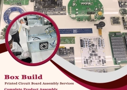
 Box Build Printed Circuit Board Assembly Services | Complete Product AssemblyFebruary 25, 2026 - 1:00 am
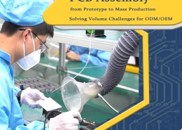
 PCB Assembly from Prototype to Mass Production: Solving Volume Challenges for ODM/OEMFebruary 10, 2026 - 1:00 am
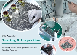
 PCB Assembly Testing & Inspection: Building Trust Through Measurable Quality ControlFebruary 5, 2026 - 1:00 am
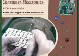
 From Prototype to Mass Production: Consumer Electronics PCB AssemblyJanuary 30, 2026 - 1:00 am
 Industrial Control PCBA Solutions With Strict DFM and MES ControlJanuary 25, 2026 - 1:00 am