PCB Assembly Testing & Inspection: How Quality Is Verified at Every Stage
1. Why PCB Assembly Testing & Inspection Matters
In PCB assembly, most failures are not design errors but process-related defects. According to IPC field data, over 60% of electronic failures originate from soldering defects, component placement errors, or insufficient process control.
(1) Discover Defects in Advance to Avoid Batch Losses
During the PCB manufacturing assembly, small welding errors or misplaced components may lead to functional failure of the entire circuit board. Through first article inspection (FAI), process accuracy can be verified before mass production, preventing a large number of defective circuit board due to design or operational errors, and significantly reducing material and labor waste. Research shows that first-piece inspection can control the defective rate below 1%, greatly improving production economy.
(2) Ensure Electrical Performance and Signal Advantages
Electrical performance testing includes continuity testing, insulation resistance testing, and signal defect analysis at high frequencies, which can identify potential problems such as open circuits, short circuits, and crosstalk. These tests not only verify that the circuit works as designed but also identify performance defects caused by improper wiring, ensuring that the PCB assembly is stable and reliable in actual applications.
(3) Improve PCB Manufacturing Reliability and Meet Strict Requirements in Application Scenarios
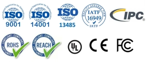
For fields with high reliability requirements such as medical care, automobiles, and industrial control, PCBs must withstand environmental reliability conditions such as temperature and humidity cycles, vibration, shock, and salt spray. This type of test simulates long-term use, evaluates the circuit board’s ability to withstand extreme environments, and ensures the service life and safety of the printed circuit board production. It is a key step in passing industry certifications (such as ISO 9001, IPC standards).
(4) Support Automated Production and Quality Traceability
Automated means such as automatic optical inspection (AOI), in-circuit testing (ICT) and functional testing (FCT) can achieve efficient and consistent quality control on SMT and DIP production lines. These tests not only detect accuracy, but also generate data records that can be supplemented and improved, while continuously optimizing the process and improving the overall manufacturing level.
(5) Comply with International Standards and Enhance Market Competitiveness
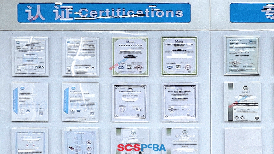
Complying with international standards such as IPC-A-610, ISO 9001, UL, ROSH etc. can not only standardize and implement quality and technology, but also help companies establish a complete quality management system. PCB boards that meet standards are more likely to earn customers’ trust and compete more effectively in the global market.
2. Industry Standards & Quality Benchmarks
Reliable PCBA testing services must rely on authoritative industry standards and strict quality benchmarks to ensure the safety, reliability and compliance of PCB board throughout the entire life cycle of design, manufacturing, assembly and application.
(1) IPC-A-610: Acceptance Standard for Electronic Components
IPC-A-610 is the most widely used assembly quality acceptance standard in the global electronics manufacturing field. It defines three-level product classification and acceptance criteria from consumer to high-reliability products.
- Class 1 (General Electronic Products)
Suitable for disposable consumer devices, allowing a certain degree of cosmetic defects. - Class 2 (dedicated service electronic products)
Used for communication equipment, industrial control, etc., requiring continuous operation but allowing limited shutdown, emphasizing functional reliability. - Class 3 (high-performance electronic products)
Suitable for high-reliability scenarios such as automotive, medical, aerospace, etc., requiring zero defect tolerance. The solder joints must be completely wetted, without voids, and without cracks.
Key inspection items include: solder joint shape, pin coplanarity, virtual soldering/bridging identification, intermetallic compound (IMC) thickness control (1–3μm), etc.
(2) IATF 16949: Automotive Process Control and Traceability
IATF 16949 is a quality management system standard unique to the automotive industry
- Implement five major tools
PPAP (Production Part Approval Process), FMEA (Failure Mode Analysis), and SPC (Statistical Process Control) - Complete process traceability, basic raw materials, process parameters, inspection records
- Must pass 1000 thermal cycle tests (-40℃ to 125℃), the gold layer does not fall off, and the contact resistance change is ≤10%
Circuit board manufacturing such as automotive light panels, ECUs, and ADAS systems must meet this standard before they can enter the OEM supply chain.
(3) UL and RoHS: Safety and Material Compliance
- UL certification (safety standards)
Verify the insulation performance, temperature resistance level, and flame retardancy of the PCB (for example, FR-4 materials need to pass UL94-V0)
Commonly used in power modules, home appliance control panels and other fields to ensure that there is no risk of fire or electric shock during use - RoHS directive (environmental protection standards)
Contents of six harmful substances including lead, heart disease, and mercury, applicable to all electronic products entering the EU market
The corresponding domestic standard is GB/T 26572, and the detection method refers to GB/T 26125 (followed by IEC 62321)
Complying with UL + RoHS at the same time means that the circuit board is both safe and environmentally friendly, improving the competitiveness in the international market.
(4) ISO Series Standards: Quality Management and Extension to Specific Industries
| ISO standard | application areas | core requirements |
|---|---|---|
| ISO 9001 | General quality management | Establish a PDCA cycle to ensure that the process is stable and controllable |
| ISO 14001 | Environmental management | Control waste emissions, energy consumption, and use of hazardous substances |
| ISO 13485 | Medical equipment | Emphasize biocompatibility, sterile processing, and traceability |
| ISO 45001 | Occupational health and safety | Ensure the safety of production personnel |
3. In-Process Inspection: SPI, AOI, X-Ray & Traceability
In the SCS PCBA circuit board assembly, the quality control of the SMT and DIP assembly processes is combined with the MES system through detection technologies such as SPI, AOI, and X-Ray to achieve full-process closed-loop control from process foundation to finished product quality.
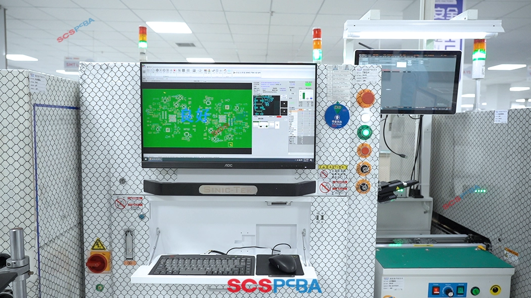
(1) 3D SPI – Solder Paste Detection
SPI (Solder Paste Inspection) performs 3D measurements of solder paste thickness, volume, and offset after printing and before patching to detect insufficient solder paste, bridging risks, and template problems to ensure a reliable welding foundation.
- The solder paste thickness is controlled at 0.1–0.15mm, and the deviation does not exceed ±10%.
- Detect defects such as less tin, more tin, bridging, and pulling points to prevent soldering or short circuits after reflow soldering.
- The BGA area is required to have a solder paste filling degree of more than 90%.
- SPI solder paste volume tolerance: ±25%
(2) AOI – Automatic Optical Inspection
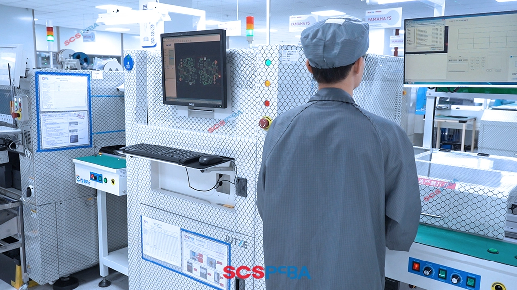
AOI (Automatic Optical Inspection) performs inspections after component placement and after reflow soldering, identifying issues such as missing components, misalignment, reversed polarity, solder bridging, and insufficient soldering.
- After component placement
Verifies correct component position, angle, and polarity. - After reflow soldering
Analyzes solder joint wetting angle, solder volume, and shape, identifying defects such as cold joints and solder balls. - AOI inspection accuracy: ≥99.5%
(3)X-Ray Inspection
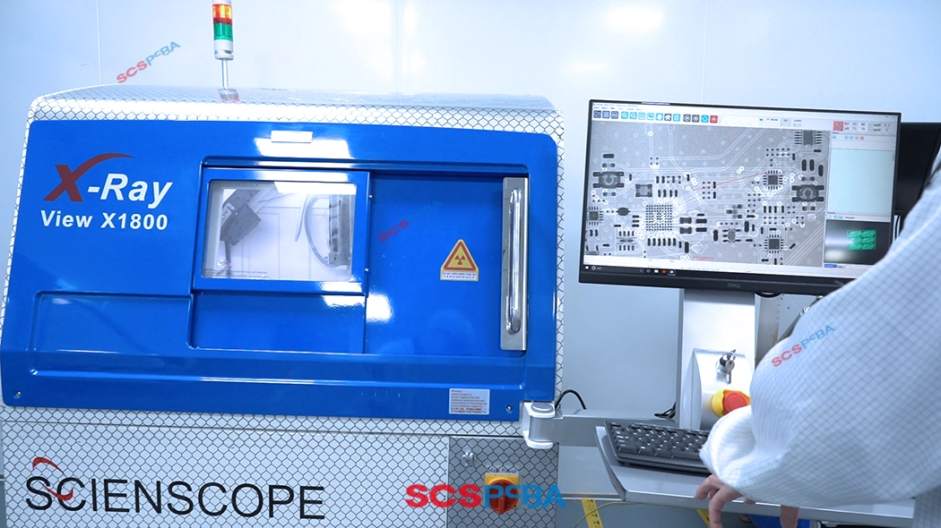
X-ray inspection is used to detect packaging types that cannot be observed with the naked eye or AOI (Automated Optical Inspection), such as bottom solder joints of BGA, CSP, and QFN packages.
- It utilizes the penetrating power of X-rays to observe solder ball integrity, void rate, and bridging.
- It can detect inter-layer connections within PCBs and damage to component packaging.
- For high-density electronic PCB assembly and manufacturing used in mobile phones and laptops, the reliability requirements for solder joints are extremely high.
(4) MES System – Full Process Traceability
The MES system integrates inspection data from SPI, AOI, and X-Ray equipment with the production process, building a complete quality data chain.
- Real-time monitoring
Collects parameters from equipment such as pick-and-place machines and reflow ovens, enabling visualization of key indicators. - Error prevention management
Scans material tray barcodes during loading, and the system automatically compares them with the BOM to prevent material errors. - Full traceability
Establishes forward and backward traceability from raw material batches → solder paste printing → component placement → testing → repair → packaging. - Data closed loop
Inspection results are automatically linked to product serial numbers, supporting anomaly alerts.
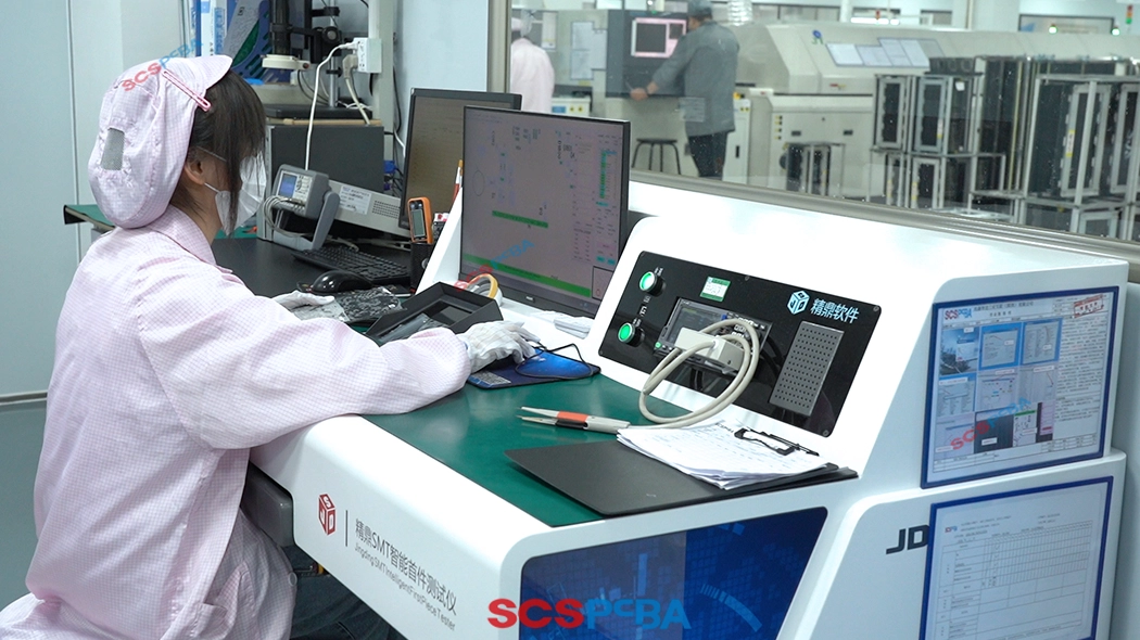
SCSPCBA introduces the MES system into the SMT process, combining it with SPI + AOI + X-Ray triple inspection. A process history file is created for each printed circuit board production, enabling precise defect location and rapid containment.
4. Functional & Reliability Testing – Which Test Fits Which Project?
Not all projects need the same testing depth.
| Test Type | Best For | Risk Coverage |
|---|---|---|
| ICT | Medium–high volume boards | Open/short, component value |
| FCT | Function-critical products | Real operating behavior |
| Burn-In | Power & industrial | Early failure screening |
| Environmental | Automotive/outdoor | Thermal & humidity stress |
5. Testing Facilities & Capability at SCSPCBA
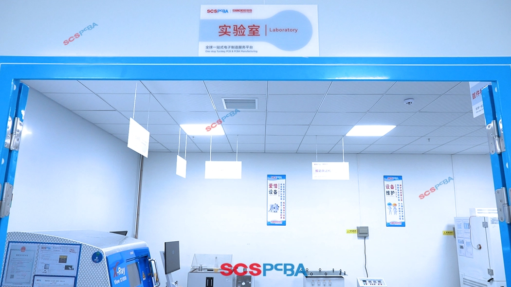
(1) Independent Testing Laboratory
SCSPCBA has established a dedicated testing laboratory independent of the PCB board production line to ensure that the testing environment is free from production interference and to achieve comprehensive quality control throughout the entire process. The laboratory adopts a partitioned management model, encompassing functional testing, environmental simulation, fault analysis, and clean repair areas. It is equipped with an intelligent monitoring system that records test data in real time and integrates with the production system.
(2) Core Testing Equipment Configuration
3D SPI System
- Utilizing laser scanning technology, it achieves precise three-dimensional measurement of solder joints with a detection accuracy of ±0.01mm, capable of identifying minute defects such as cold solder joints and short circuits.
- Integrated with AI algorithms, it automatically compares the design model with the actual welding results and generates a visual quality report.
High-Resolution AOI Inspection Line
- Equipped with a 4K industrial camera and multi-spectral imaging technology, it performs full inspection of the circuit board manufacturing surface, identifying defects such as scratches, oxidation, and component misalignment, with a false negative rate of less than 0.01%.
- Supports automatic storage and classification of NG (Not Good) images, facilitating root cause analysis of defects.
X-ray Inspection Machine
- Using a microfocus X-ray source and flat panel detector, it achieves non-destructive testing of the internal structure of BGA, CSP, and other packaging forms, with a resolution of 5μm.
- Integrates automatic defect marking function, accurately locating hidden defects such as voids and cracks.
ICT and FCT Test Stations
- The ICT (In-Circuit Test) system verifies the electrical performance of circuit board through probe contact testing, supporting mixed-signal testing of analog and digital circuits.
- The FCT (Functional Test) platform simulates the actual working environment, performing aging tests and functional verification on finished products to ensure product reliability.
Environmental Simulation Equipment
- Vibration Testing Machine
Simulates mechanical stress during transportation and use, with a test frequency range of 0-5kHz and acceleration up to 10g. - Temperature and Humidity Test Chamber
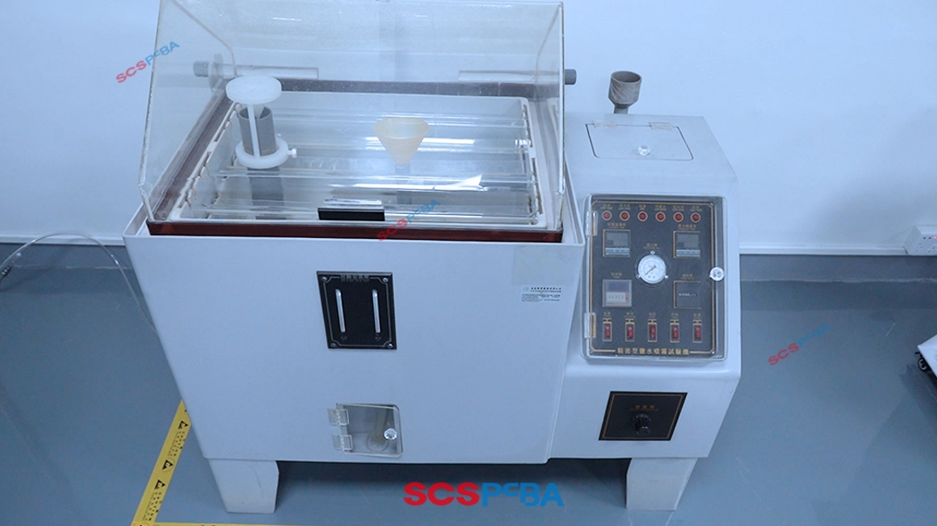
Covers a temperature range of -40℃ to +125℃, with humidity control accuracy of ±2%, used for accelerated aging testing. - Salt Spray Test Chamber
Complies with GB/T 2423.17 standard, simulating corrosion in coastal environments, with adjustable test cycles.
Fault Analysis and Repair Facilities
- Equipped with Class 100 clean workstations and anti-static equipment, supporting tools such as microscopes and X-ray flaw detectors for defect localization and repair.
- The repair process is controlled by SOP (Standard Operating Procedures) to ensure that repaired printed circuit board assembly services meet the original design requirements.
(3) Quality Control System
Layered Inspection Mechanism
- First Article Inspection (FAI)
A full-item inspection of the first produced unit is conducted before mass PCB board production begins to confirm that process parameters are consistent with design requirements. - In-Process Quality Control (IPQC)
Sampling inspections are conducted after key processes such as SMT placement and wave soldering to intercept defects in real time. - Outgoing Quality Assurance (OQA)
100% functional testing and visual inspection are performed before finished products are shipped to ensure zero-defect delivery.
Defect Closed-Loop Management
- Real-time defect data is collected through the MES (Manufacturing Execution System), automatically triggering alerts and sending them to the relevant personnel.
- A defect database is established to analyze high-frequency problems and to drive optimization of the printed circuit board manufacturing process and adjustments to equipment parameters.
- PCB circuit board requiring rework must undergo secondary testing to ensure that the problems are completely resolved, forming a closed loop of “discovery-analysis-improvement-verification.”
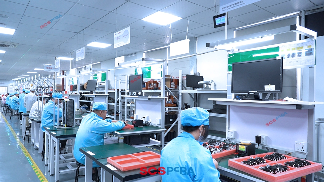
6. SCSPCBA PCB Assembly and Testing: The Complete Process
PCB assembly and testing are not single processes but rather a multi-level quality control system that spans the entire process from raw material warehousing to finished product shipment. The following is SCSPCBA’s core testing process:
(1) PCB Raw Material Incoming Inspection
- PCB Substrate
Inspect for surface contamination, scratches, deformation, hole position accuracy, and impedance matching. - PCB Board Components
Verify model number, polarity, and package dimensions; check for compliance with moisture sensitivity level (MSL). - Solder Paste and Flux
Verify viscosity, metal content, activity, and storage conditions.
Common tools: Optical microscope, automatic optical inspection (AOI) system, hygrometer
(2) PCB Manufacturing Process monitoring
| Manufacturing Process | Inspection Items |
|---|---|
| Solder paste printing | Printing thickness, misalignment, leakage, blurring |
| SMT Assembly | Component presence/absence, positional deviation, polarity reversal, and lifting/tilting |
| Reflow soldering | Temperature profile monitoring, wettability, bridging, cold solder joints |
| Wave soldering | Solder joint fullness, solder penetration rate, shadowing effect |
Real-time monitoring can effectively intercept over 90% of early-stage defects.
(3) Post-Assembly Testing
- Visual Inspection
Using AOI (Automated Optical Inspection) to check solder joint quality, missing or misplaced components. - Electrical Performance Testing
- In-Circuit Test (ICT): Using a test fixture to detect open circuits and short circuits.
- Flying Probe Test: Suitable for small batches and high-density boards.
- Functional Test (FCT)
Simulating the actual working environment to verify overall system performance. - X-ray Inspection
Used for quality assessment of hidden solder joints such as BGA and QFN.
(4) Reliability Verification Testing
- Temperature and humidity cycling test (-40℃~+85℃)
- Vibration and shock testing
- Salt spray test (applicable to outdoor equipment)
- High-temperature aging test (Burn-in)
(5) OQA Inspection and Final Approval
(6) Packaging and Shipment Traceability
These tests ensure the long-term stable operation of the PCB board assembly in complex environments and form the basis for certifications such as ISO 9001 and IATF 16949.

7. How to choose the right PCB/PCBA testing method?
(1) PCB Manufacturing (Bare Board Stage)
- Open/Short Circuit Test
Using flying probes or test fixtures, verify the continuity and insulation of the traces to ensure there are no open or short circuits. Applicable to all PCBs, this is a fundamental and mandatory test. - Impedance Test
For high-speed signal lines (such as USB and HDMI), measure the characteristic impedance using a TDR to ensure it meets design tolerances (typically ±10%). - High Voltage Withstand Test (Hi-Pot)
Apply 500V DC for 30 seconds to high-voltage boards (such as power modules) to test interlayer insulation performance.
(2) Post-Assembly (PCBA Stage)
- AOI (Automated Optical Inspection)
Uses multi-angle cameras to scan solder joints and component positions, identifying surface defects such as missing components, misaligned components, misalignment, and bridging. Suitable for mass production, but cannot inspect BGA bottom solder joints. - ICT (In-Circuit Testing)
Uses a bed of probes to contact test points, measuring resistance, capacitance, and polarity to locate component-level faults. High accuracy and coverage exceeding 95%, but requires custom fixtures; suitable for large-volume orders. - Flying Probe Testing
Moves probes to sequentially contact test points, requiring no fixtures; suitable for prototyping or small-batch production. Disadvantages include slow speed and unsuitability for high-density boards. - Automated X-ray Inspection
Specifically designed for hidden packages such as BGA and QFN, detecting solder voids, cold solder joints, and internal short circuits. A critical step in automotive electronics and medical equipment.
(3) Functional and Reliability Verification
- FCT (Functional Testing)
Simulates actual working conditions to verify the overall board functionality (e.g., communication interfaces, software operation). - Environmental Stress Testing
- Temperature Cycling
Cycling from -40℃ to 125℃ to examine the risk of fracture due to thermal expansion and contraction. - Vibration Testing
1 hour each along the X/Y/Z axes to assess vibration resistance. - High Temperature and High Humidity Testing
Running for several days in an 85°C/85%RH environment to accelerate aging and assess lifespan.
- Temperature Cycling
- Burn-in Testing
Running for 48-72 hours with power on to prematurely expose components prone to “early failure,” improving the reliability of circuit board manufacturing leaving the factory.
(4) Test Items in Different Application Fields
| Application areas | core standards | Test items |
|---|---|---|
| Automotive electronics | IATF 16949 + IPC-A-610 Class 3 | Thermal cycling, vibration, salt spray, PPAP files |
| Medical equipment | ISO 13485 + ISO 10993 + IPC-A-610 | Ionic contamination, chemical resistance, and biocompatibility |
| Industrial control | IPC-A-610 Class 2 + ISO 9001 | Continuity test, insulation resistance, high temperature aging |
| Aerospace | MIL-P-45204 + IPC-A-610 Class 3 | Gold layer thickness ≥0.76μm, no corrosion in salt spray for 96 hours |
| Outdoor communications | IEC 60068-2-30 + ISO 9227 | Temperature and humidity cycle, UV aging, salt spray test |
- Mass Printed Circuit Board Production
Prioritize ICT+FCT. Although initial investment is high, the unit cost is low and efficiency is high. - Prototyping or R&D Stage
Use flying probes instead of ICT to save on fixture manufacturing time and costs.

